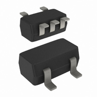
74AHC1G125GW,125 NXP Semiconductors, 74AHC1G125GW,125 Datasheet - Page 2

74AHC1G125GW,125
Manufacturer Part Number
74AHC1G125GW,125
Description
IC BUS BUFF DVR TRI-ST 5TSSOP
Manufacturer
NXP Semiconductors
Series
74AHCr
Datasheet
1.74AHCT1G125GW125.pdf
(16 pages)
Specifications of 74AHC1G125GW,125
Package / Case
SC-70-5, SC-88A, SOT-323-5, SOT-353, 5-TSSOP
Logic Type
Buffer/Line Driver, Non-Inverting
Number Of Elements
1
Number Of Bits Per Element
1
Current - Output High, Low
8mA, 8mA
Voltage - Supply
2 V ~ 5.5 V
Operating Temperature
-40°C ~ 125°C
Mounting Type
Surface Mount
Logic Family
AHC
Number Of Channels Per Chip
1
Polarity
Non-Inverting
Supply Voltage (max)
5.5 V
Supply Voltage (min)
2 V
Maximum Operating Temperature
+ 125 C
Mounting Style
SMD/SMT
High Level Output Current
- 8 mA
Input Bias Current (max)
1 uA
Low Level Output Current
8 mA
Minimum Operating Temperature
- 40 C
Output Type
3-State
Propagation Delay Time
11.5 ns @ 3 V to 3.6 V or 7.5 ns @ 4.5 V to 5.5 V
Number Of Lines (input / Output)
1 / 1
Logical Function
Buffer/Line Driver
Number Of Elements
1
Number Of Channels
1
Number Of Inputs
1
Number Of Outputs
1
Operating Supply Voltage (typ)
5V
Package Type
TSSOP
Operating Supply Voltage (max)
5.5V
Operating Supply Voltage (min)
2V
Quiescent Current
1uA
Technology
CMOS
Pin Count
5
Mounting
Surface Mount
Operating Temp Range
-40C to 125C
Operating Temperature Classification
Automotive
Lead Free Status / RoHS Status
Lead free / RoHS Compliant
Lead Free Status / RoHS Status
Lead free / RoHS Compliant, Lead free / RoHS Compliant
Other names
568-4452-2
74AHC1G125GW-G
74AHC1G125GW-G
935263002125
74AHC1G125GW-G
74AHC1G125GW-G
935263002125
Available stocks
Company
Part Number
Manufacturer
Quantity
Price
Company:
Part Number:
74AHC1G125GW,125
Manufacturer:
NXP Semiconductors
Quantity:
4 750
NXP Semiconductors
4. Marking
Table 2.
[1]
5. Functional diagram
6. Pinning information
74AHC_AHCT1G125_9
Product data sheet
Type number
74AHC1G125GW
74AHCT1G125GW
74AHC1G125GV
74AHCT1G125GV
74AHC1G125GM
74AHCT1G125GM
74AHC1G125GF
74AHCT1G125GF
Fig 1.
Fig 4.
The pin 1 indicator is located on the lower left corner of the device, below the marking code.
GND
OE
2
1
A
Logic symbol
Pin configuration
SOT353-1 and SOT753
Marking codes
1
2
3
OE
A
74AHCT1G125
74AHC1G125
6.1 Pinning
001aaf101
mna118
Y
5
4
4
V
Y
CC
Fig 2.
Fig 5.
GND
Rev. 09 — 22 June 2009
2
1
OE
IEC logic symbol
Pin configuration SOT886
A
Transparent top view
74AHC1G125; 74AHCT1G125
74AHCT1G125
74AHC1G125
EN
1
2
3
Marking
AM
CM
A25
C25
AM
CM
AM
CM
mna119
001aaj971
6
5
4
V
n.c.
Y
[1]
CC
4
Fig 3.
Fig 6.
OE
A
Bus buffer/line driver; 3-state
GND
OE
Logic diagram
Pin configuration SOT891
A
Transparent top view
74AHCT1G125
74AHC1G125
1
2
3
© NXP B.V. 2009. All rights reserved.
001aaj972
6
5
4
V
n.c.
Y
CC
mna120
2 of 16
Y


