74AUP1G126GM,115 NXP Semiconductors, 74AUP1G126GM,115 Datasheet - Page 11
74AUP1G126GM,115
Manufacturer Part Number
74AUP1G126GM,115
Description
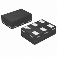
IC BUFF DVR TRI-ST LOW PWR 6XSON
Manufacturer
NXP Semiconductors
Series
74AUPr
Datasheet
1.74AUP1G126GW125.pdf
(24 pages)
Specifications of 74AUP1G126GM,115
Logic Type
Buffer/Line Driver, Non-Inverting
Number Of Elements
1
Number Of Bits Per Element
1
Current - Output High, Low
4mA, 4mA
Voltage - Supply
0.8 V ~ 3.6 V
Operating Temperature
-40°C ~ 125°C
Mounting Type
Surface Mount
Package / Case
6-XSON (Micropak™), SOT-886
Logic Family
AUP
Number Of Channels Per Chip
1
Polarity
Non-Inverting
Supply Voltage (max)
3.6 V
Supply Voltage (min)
0.8 V
Maximum Operating Temperature
+ 125 C
Mounting Style
SMD/SMT
High Level Output Current
- 4 mA
Low Level Output Current
4 mA
Minimum Operating Temperature
- 40 C
Number Of Lines (input / Output)
1 / 1
Output Type
3-State
Propagation Delay Time
18.7 ns at 1.1 V to 1.3 V, 10.8 ns at 1.4 V to 1.6 V, 8.4 ns at 1.65 V to 1.95 V, 6.3 ns at 2.3 V to 2.7 V, 5.8 ns at 3 V to 3.6 V
Lead Free Status / RoHS Status
Lead free / RoHS Compliant
Other names
568-2556-2
935279057115
935279057115


NXP Semiconductors
Table 8.
Voltages are referenced to GND (ground = 0 V); for test circuit see
[1]
[2]
[3]
[4]
[5]
Table 9.
Voltages are referenced to GND (ground = 0 V); for test circuit see
74AUP1G126
Product data sheet
Symbol
T
C
Symbol
C
t
t
pd
en
amb
PD
L
= 5 pF
All typical values are measured at nominal V
t
t
t
C
P
f
f
C
V
N = number of inputs switching;
Σ(C
pd
en
dis
i
o
D
CC
= 25 °C
PD
= input frequency in MHz;
L
= output frequency in MHz;
is the same as t
is the same as t
= output load capacitance in pF;
= C
is the same as t
L
is used to determine the dynamic power dissipation (P
= supply voltage in V;
× V
PD
Parameter
propagation delay
enable time
Dynamic characteristics
Dynamic characteristics
CC
Parameter
power dissipation capacitance f = 1 MHz; V
× V
2
× f
CC
o
2
) = sum of the outputs.
× f
PLH
PZH
PHZ
i
× N + Σ(C
and t
and t
and t
PHL
PZL
PLZ
L
.
.
.
× V
CC
Conditions
A to Y; see
OE to Y; see
2
…continued
V
V
V
V
V
V
V
V
V
V
× f
CC
CC
CC
CC
CC
CC
CC
CC
CC
CC
o
All information provided in this document is subject to legal disclaimers.
) where:
= 1.1 V to 1.3 V
= 1.4 V to 1.6 V
= 1.65 V to 1.95 V
= 2.3 V to 2.7 V
= 3.0 V to 3.6 V
= 1.1 V to 1.3 V
= 1.4 V to 1.6 V
= 1.65 V to 1.95 V
= 2.3 V to 2.7 V
= 3.0 V to 3.6 V
CC
Conditions
output enabled
.
V
V
V
V
V
V
CC
CC
CC
CC
CC
CC
Figure 7
Rev. 3 — 3 September 2010
Figure 8
= 0.8 V
= 1.1 V to 1.3 V
= 1.4 V to 1.6 V
= 1.65 V to 1.95 V
= 2.3 V to 2.7 V
= 3.0 V to 3.6 V
D
I
= GND to V
in μW).
Figure 9
Figure 9
[1]
[2]
CC
−40 °C to +85 °C
Min
2.5
2.0
1.7
1.4
1.2
2.6
2.2
1.7
1.4
1.2
[5]
Min
-
-
-
-
-
-
Low-power buffer/line driver; 3-state
Max
13.6
11.7
7.3
6.1
4.3
3.9
7.4
5.9
3.8
3.2
Typ
2.7
2.8
2.9
3.0
3.6
4.2
74AUP1G126
−40 °C to +125 °C
Min
[1]
2.5
2.0
1.7
1.4
1.2
2.6
2.2
1.7
1.4
1.2
Max
-
-
-
-
-
-
© NXP B.V. 2010. All rights reserved.
Max
12.9
13.6
8.1
6.7
4.9
4.4
7.7
6.2
4.1
3.4
Unit
pF
pF
pF
pF
pF
pF
Unit
ns
ns
ns
ns
ns
ns
ns
ns
ns
ns
11 of 24
Related parts for 74AUP1G126GM,115
Image
Part Number
Description
Manufacturer
Datasheet
Request
R

Part Number:
Description:
NXP Semiconductors designed the LPC2420/2460 microcontroller around a 16-bit/32-bitARM7TDMI-S CPU core with real-time debug interfaces that include both JTAG andembedded trace
Manufacturer:
NXP Semiconductors
Datasheet:

Part Number:
Description:
NXP Semiconductors designed the LPC2458 microcontroller around a 16-bit/32-bitARM7TDMI-S CPU core with real-time debug interfaces that include both JTAG andembedded trace
Manufacturer:
NXP Semiconductors
Datasheet:
Part Number:
Description:
NXP Semiconductors designed the LPC2468 microcontroller around a 16-bit/32-bitARM7TDMI-S CPU core with real-time debug interfaces that include both JTAG andembedded trace
Manufacturer:
NXP Semiconductors
Datasheet:
Part Number:
Description:
NXP Semiconductors designed the LPC2470 microcontroller, powered by theARM7TDMI-S core, to be a highly integrated microcontroller for a wide range ofapplications that require advanced communications and high quality graphic displays
Manufacturer:
NXP Semiconductors
Datasheet:
Part Number:
Description:
NXP Semiconductors designed the LPC2478 microcontroller, powered by theARM7TDMI-S core, to be a highly integrated microcontroller for a wide range ofapplications that require advanced communications and high quality graphic displays
Manufacturer:
NXP Semiconductors
Datasheet:
Part Number:
Description:
The Philips Semiconductors XA (eXtended Architecture) family of 16-bit single-chip microcontrollers is powerful enough to easily handle the requirements of high performance embedded applications, yet inexpensive enough to compete in the market for hi
Manufacturer:
NXP Semiconductors
Datasheet:
Part Number:
Description:
The XA-S3 device is a member of Philips Semiconductors? XA(eXtended Architecture) family of high performance 16-bitsingle-chip microcontrollers
Manufacturer:
NXP Semiconductors
Datasheet:

Part Number:
Description:
The NXP BlueStreak LH75401/LH75411 family consists of two low-cost 16/32-bit System-on-Chip (SoC) devices
Manufacturer:
NXP Semiconductors
Datasheet:
Part Number:
Description:
The NXP LPC3130/3131 combine an 180 MHz ARM926EJ-S CPU core, high-speed USB2
Manufacturer:
NXP Semiconductors
Datasheet:
Part Number:
Description:
The NXP LPC3141 combine a 270 MHz ARM926EJ-S CPU core, High-speed USB 2
Manufacturer:
NXP Semiconductors
Part Number:
Description:
The NXP LPC3143 combine a 270 MHz ARM926EJ-S CPU core, High-speed USB 2
Manufacturer:
NXP Semiconductors

Part Number:
Description:
The NXP LPC3152 combines an 180 MHz ARM926EJ-S CPU core, High-speed USB 2
Manufacturer:
NXP Semiconductors
Part Number:
Description:
The NXP LPC3154 combines an 180 MHz ARM926EJ-S CPU core, High-speed USB 2
Manufacturer:
NXP Semiconductors

Part Number:
Description:
Standard level N-channel enhancement mode Field-Effect Transistor (FET) in a plastic package using NXP High-Performance Automotive (HPA) TrenchMOS technology
Manufacturer:
NXP Semiconductors
Datasheet: