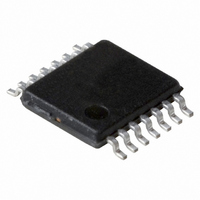
74LVC07APW,112 NXP Semiconductors, 74LVC07APW,112 Datasheet - Page 9

74LVC07APW,112
Manufacturer Part Number
74LVC07APW,112
Description
IC BUFF HEX OPEN DRAIN 14TSSOP
Manufacturer
NXP Semiconductors
Series
74LVCr
Datasheet
1.74LVC07ABQ115.pdf
(14 pages)
Specifications of 74LVC07APW,112
Logic Type
Buffer/Line Driver, Non-Inverting with Open Drain
Number Of Elements
6
Number Of Bits Per Element
1
Current - Output High, Low
32mA, 32mA
Voltage - Supply
2 V ~ 5.5 V
Operating Temperature
-40°C ~ 125°C
Mounting Type
Surface Mount
Package / Case
14-TSSOP
Logic Family
LVC
Number Of Channels Per Chip
6
Polarity
Non-Inverting
Supply Voltage (max)
5.5 V
Supply Voltage (min)
1.65 V
Maximum Operating Temperature
+ 125 C
Mounting Style
SMD/SMT
Low Level Output Current
32 mA
Minimum Operating Temperature
- 40 C
Number Of Lines (input / Output)
6 / 6
Output Type
Open Drain
Propagation Delay Time
2.4 ns at 2.7 V, 2.2 ns at 3.3 V, 1.6 ns at 5 V
Lead Free Status / RoHS Status
Lead free / RoHS Compliant
Other names
74LVC07APW
74LVC07APW
935265482112
74LVC07APW
935265482112
Philips Semiconductors
AC WAVEFORMS
2003 Nov 11
handbook, full pagewidth
handbook, full pagewidth
Hex buffer with open-drain outputs
Definitions for test circuits:
R
C
R
<2.7 V
1.65 to 1.95 V
2.3 to 2.7 V
2.7 V
3.0 to 3.6 V
4.5 to 5.5 V
L
L
T
2.7 to 3.6 V
4.5 to 5.5 V
= Load resistor.
= Load capacitance including jig and probe capacitance.
= Termination resistance should be equal to the output impedance Z
V
CC
V
CC
0.5
1.5 V
0.5
2
2
6 V
6 V
2
V
V
V
V
CC
CC
V
V
V
M
ext
CC
CC
CC
nA input
nY output
Fig.6 The input nA to output nY propagation delays.
MNA530
GENERATOR
GND
V CC
V
V
2.7 V
2.7 V
V
V OL
V
V
V
CC
CC
CC
V I
OL
OL
OL
PULSE
Fig.7 Load circuitry for switching times.
V
+ 0.15 V
+ 0.3 V
+ 0.3 V
I
V
X
V M
t PLZ
30 pF
30 pF
50 pF
50 pF
50 pF
V I
C
L
o
R T
V X
of the pulse generator.
9
D.U.T.
V CC
1 k
500
500
500
500
R
V O
L
t PZL
C L
V ext
R L
R L
V M
MNA528
Product specification
74LVC07A


