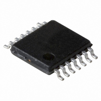
74LVC125APW,118 NXP Semiconductors, 74LVC125APW,118 Datasheet - Page 3

74LVC125APW,118
Manufacturer Part Number
74LVC125APW,118
Description
IC BUFF DVR TRI-ST QD 14TSSOP
Manufacturer
NXP Semiconductors
Series
74LVCr
Datasheet
1.74LVC125ABQ115.pdf
(20 pages)
Specifications of 74LVC125APW,118
Package / Case
14-TSSOP
Logic Type
Buffer/Line Driver, Non-Inverting
Number Of Elements
4
Number Of Bits Per Element
1
Current - Output High, Low
24mA, 24mA
Voltage - Supply
2.7 V ~ 3.6 V
Operating Temperature
-40°C ~ 125°C
Mounting Type
Surface Mount
Logic Family
LVC
Number Of Channels Per Chip
4
Polarity
Non-Inverting
Supply Voltage (max)
3.6 V
Supply Voltage (min)
1.2 V
Maximum Operating Temperature
+ 125 C
Mounting Style
SMD/SMT
High Level Output Current
- 24 mA
Input Bias Current (max)
40 uA
Low Level Output Current
24 mA
Minimum Operating Temperature
- 40 C
Output Type
3-State
Propagation Delay Time
2.4 ns (Typ) @ 3.3 V
Number Of Lines (input / Output)
4 / 4
Logical Function
Buffer/Line Driver
Number Of Elements
4
Number Of Channels
4
Number Of Inputs
4
Number Of Outputs
4
Operating Supply Voltage (typ)
1.8/2.5/3.3V
Package Type
TSSOP
Operating Supply Voltage (max)
3.6V
Operating Supply Voltage (min)
1.2V
Quiescent Current
40uA
Technology
CMOS
Pin Count
14
Mounting
Surface Mount
Operating Temp Range
-40C to 125C
Operating Temperature Classification
Automotive
Lead Free Status / RoHS Status
Lead free / RoHS Compliant
Lead Free Status / RoHS Status
Lead free / RoHS Compliant, Lead free / RoHS Compliant
Other names
568-2288-2
74LVC125APW-T
935231720118
74LVC125APW-T
935231720118
Philips Semiconductors
FUNCTION TABLE
See note 1.
Note
1. H = HIGH voltage level;
PINNING
2003 May 07
Quad buffer/line driver with 5 V tolerant input/outputs;
3-state
L = LOW voltage level;
X = don’t care;
Z = high-impedance OFF-state.
PIN
10
11
12
13
14
1
2
3
4
5
6
7
8
9
1OE
1A
1Y
2OE
2A
2Y
GND
3Y
3A
3OE
4Y
4A
4OE
V
SYMBOL
CC
nOE
H
L
L
data enable input (active LOW)
data input
data output
data enable input (active LOW)
data input
data output
ground (0 V)
data output
data input
data enable input (active LOW)
data output
data input
data enable input (active LOW)
supply voltage
DESCRIPTION
INPUT
nA
H
X
L
3
Fig.1 Pin configuration SO14 and (T)SSOP14.
GND
1OE
2OE
1A
1Y
2A
2Y
1
2
3
4
5
6
7
125
MNA226
OUTPUT
14
13
12
11
10
9
8
nY
Product specification
H
Z
74LVC125A
L
V CC
4OE
4A
4Y
3OE
3A
3Y


