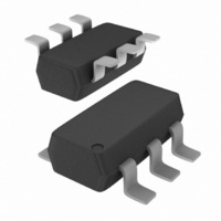
74HCT2G17GV,125 NXP Semiconductors, 74HCT2G17GV,125 Datasheet - Page 13

74HCT2G17GV,125
Manufacturer Part Number
74HCT2G17GV,125
Description
IC BUFF DL SCHM TRG N-INV 6TSOP
Manufacturer
NXP Semiconductors
Series
74HCTr
Datasheet
1.74HCT2G17GW125.pdf
(22 pages)
Specifications of 74HCT2G17GV,125
Logic Type
Schmitt Trigger - Buffer, Driver
Number Of Elements
2
Number Of Bits Per Element
1
Current - Output High, Low
4mA, 4mA
Voltage - Supply
4.5 V ~ 5.5 V
Operating Temperature
-40°C ~ 125°C
Mounting Type
Surface Mount
Package / Case
SC-74-6
Logic Family
HCT
Number Of Channels Per Chip
2
Polarity
Non-Inverting
Supply Voltage (max)
5.5 V
Supply Voltage (min)
4.5 V
Maximum Operating Temperature
+ 125 C
Mounting Style
SMD/SMT
High Level Output Current
- 4 mA
Low Level Output Current
4 mA
Maximum Power Dissipation
250 mW
Minimum Operating Temperature
- 40 C
Number Of Lines (input / Output)
2 / 2
Propagation Delay Time
45 ns
Lead Free Status / RoHS Status
Lead free / RoHS Compliant
Other names
74HCT2G17GV-G
74HCT2G17GV-G
935281028125
74HCT2G17GV-G
935281028125
Philips Semiconductors
AC WAVEFORMS
2003 Jul 10
handbook, full pagewidth
Dual D-type flip-flop with set and reset;
positive-edge trigger
The shaded areas indicate when the input is permitted to change for predictable output performance.
74HC74: V
74HCT74: V
Fig.7
The clock (nCP) to output (nQ, nQ) propagation delays, the clock pulse width, the nD to nCP set-up,
the nCP to nD hold times, the output transition times and the maximum clock pulse frequency.
M
M
= 50%; V
= 1.3 V; V
I
= GND to V
I
= GND to 3 V.
nCP input
nQ output
nQ output
nD input
CC
.
GND
GND
V OH
V OH
V OL
V OL
V I
V I
V M
t PLH
t su
t h
V M
13
V M
t W
V M
t PHL
1/f max
t PHL
t su
t h
t PLH
MNA422
74HC74; 74HCT74
Product specification


