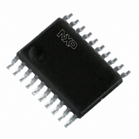
74LVCH244APW,112 NXP Semiconductors, 74LVCH244APW,112 Datasheet - Page 8

74LVCH244APW,112
Manufacturer Part Number
74LVCH244APW,112
Description
IC BUFF/DVR TRI-ST DUAL 20TSSOP
Manufacturer
NXP Semiconductors
Series
74LVCHr
Datasheet
1.74LVC244APW118.pdf
(18 pages)
Specifications of 74LVCH244APW,112
Logic Type
Buffer/Line Driver, Non-Inverting
Number Of Elements
2
Number Of Bits Per Element
4
Current - Output High, Low
24mA, 24mA
Voltage - Supply
1.2 V ~ 3.6 V
Operating Temperature
-40°C ~ 125°C
Mounting Type
Surface Mount
Package / Case
20-TSSOP
Logic Family
LVC
Logical Function
Buffer/Line Driver
Number Of Elements
2
Number Of Channels
8
Number Of Inputs
8
Number Of Outputs
8
Operating Supply Voltage (typ)
1.8/2.5/3.3V
Package Type
TSSOP
Output Type
3-State
Polarity
Non-Inverting
Propagation Delay Time
11ns
High Level Output Current
-24mA
Low Level Output Current
24mA
Operating Supply Voltage (max)
3.6V
Operating Supply Voltage (min)
1.2V
Quiescent Current
40uA
Technology
CMOS
Pin Count
20
Mounting
Surface Mount
Operating Temp Range
-40C to 125C
Operating Temperature Classification
Automotive
Lead Free Status / RoHS Status
Lead free / RoHS Compliant
Other names
74LVCH244APW
74LVCH244APW
935210350112
74LVCH244APW
935210350112
NXP Semiconductors
Table 7.
Voltages are referenced to GND (ground = 0 V). For test circuit see
[1]
[2]
[3]
[4]
[5]
11. AC waveforms
74LVC_LVCH244A_6
Product data sheet
Symbol Parameter
C
Fig 6.
PD
t
t
t
Typical values are measured at T
Typical values are measured at T
Skew between any two outputs of the same package switching in the same direction. This parameter is guaranteed by design.
C
P
f
C
V
N = number of inputs switching
pd
en
dis
i
(C
D
CC
PD
= input frequency in MHz; f
L
is the same as t
is the same as t
= output load capacitance in pF
is the same as t
= C
L
is used to determine the dynamic power dissipation (P
= supply voltage in Volts
power
dissipation
capacitance
Measurement points are given in
Logic levels: V
The input (nAn) to output (nYn) propagation delays
PD
V
Dynamic characteristics
CC
2
V
CC
f
o
2
) = sum of the outputs.
PLH
PZL
f
PLZ
i
OL
and t
N + (C
and t
and t
and V
Conditions
per buffer; V
PZH
PHL
PHZ
o
OH
= output frequency in MHz
L
.
.
.
amb
amb
are typical output voltage levels that occur with the output load.
V
CC
nYn output
= 25 C.
= 25 C and V
nAn input
2
…continued
I
= GND to V
Table
f
o
) where:
GND
V
V
8.
OH
OL
V
I
Rev. 06 — 13 August 2009
CC
t
PLH
CC
= 3.3 V.
; V
CC
D
V
in W).
M
= 3.3 V
V
M
74LVC244A; 74LVCH244A
Figure
[5]
Min
8.
-
V
40 C to +85 C
M
V
M
t
Typ
PHL
mna171
10
[2]
Octal buffer/line driver; 3-state
Max
-
40 C to +125 C Unit
Min
-
© NXP B.V. 2009. All rights reserved.
Max
-
8 of 18
pF


