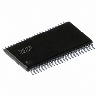
74LVC16245ADGG,118 NXP Semiconductors, 74LVC16245ADGG,118 Datasheet - Page 10

74LVC16245ADGG,118
Manufacturer Part Number
74LVC16245ADGG,118
Description
IC BUS TRCVR 3-ST 16BIT 48TSSOP
Manufacturer
NXP Semiconductors
Series
74LVCr
Specifications of 74LVC16245ADGG,118
Logic Type
Transceiver, Non-Inverting
Package / Case
48-TSSOP
Number Of Elements
2
Number Of Bits Per Element
8
Current - Output High, Low
24mA, 24mA
Voltage - Supply
1.2 V ~ 3.6 V
Operating Temperature
-40°C ~ 125°C
Mounting Type
Surface Mount
Logic Family
LVC
Number Of Channels Per Chip
16
Input Level
LVTTL
Output Level
LVTTL
Output Type
3-State
High Level Output Current
- 24 mA
Low Level Output Current
24 mA
Propagation Delay Time
2.2 ns
Supply Voltage (max)
3.6 V
Supply Voltage (min)
1.2 V
Maximum Operating Temperature
+ 125 C
Function
Bus Transceiver
Input Bias Current (max)
40 uA
Minimum Operating Temperature
- 40 C
Mounting Style
SMD/SMT
Polarity
Non-Inverting
Number Of Circuits
2
Operating Supply Voltage (typ)
1.8/2.5/3.3V
Number Of Elements
2
Number Of Channels
16
Input Logic Level
LVTTL
Output Logic Level
LVTTL
Logical Function
Bus Transceiver
Operating Supply Voltage (min)
1.2V
Quiescent Current (typ)
100nA
Technology
CMOS
Operating Temp Range
-40C to 125C
Operating Temperature Classification
Automotive
Mounting
Surface Mount
Pin Count
48
Lead Free Status / RoHS Status
Lead free / RoHS Compliant
Lead Free Status / RoHS Status
Lead free / RoHS Compliant, Lead free / RoHS Compliant
Other names
568-2292-2
74LVC16245ADG-T
74LVC16245ADGG,518
935235090518
74LVC16245ADG-T
74LVC16245ADGG,518
935235090518
NXP Semiconductors
Table 7.
Voltages are referenced to GND (ground = 0 V). For test circuit see
[1]
[2]
[3]
11. Waveforms
74LVC_LVCH16245A_9
Product data sheet
Symbol Parameter
C
Fig 7.
PD
t
t
t
Typical values are measured at T
C
P
f
C
V
N = number of inputs switching
Σ(C
pd
en
dis
i
D
CC
PD
= input frequency in MHz; f
L
is the same as t
is the same as t
= output load capacitance in pF
= C
is the same as t
L
is used to determine the dynamic power dissipation (P
= supply voltage in Volts
× V
power
dissipation
capacitance
Measurement points are given in
Logic levels: V
The input (nAn, nBn) to output (nBn, nAn) propagation delays
PD
Dynamic characteristics
CC
× V
2
× f
CC
o
2
) = sum of the outputs.
× f
PLH
PZL
PLZ
i
× N + Σ(C
OL
and t
and t
and t
and V
Conditions
per buffer; V
V
CC
PZH
PHL
PHZ
o
= 3.3 V
= output frequency in MHz
OH
L
.
.
.
× V
amb
are typical output voltage levels that occur with the output load.
CC
nAn, nBn
nBn, nAn
= 25 °C and V
output
2
input
…continued
I
× f
= GND to V
Table
o
All information provided in this document is subject to legal disclaimers.
) where:
GND
V
V
OH
8.
OL
V
I
CC
Rev. 09 — 29 March 2010
t
CC
PHL
74LVC16245A; 74LVCH16245A
16-bit bus transceiver with direction pin; 5 V tolerant; 3-state
= 3.3 V.
;
D
in μW).
V
M
V
M
[3]
Figure
Min
-
−40 °C to +85 °C
9.
Typ
30
t
mna477
PLH
Max
-
−40 °C to +125 °C Unit
Min
-
© NXP B.V. 2010. All rights reserved.
Max
-
10 of 20
pF


