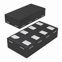
74LVC2G125GT,115 NXP Semiconductors, 74LVC2G125GT,115 Datasheet - Page 2

74LVC2G125GT,115
Manufacturer Part Number
74LVC2G125GT,115
Description
IC BUS BUFF DVR TRI-ST DL 8XSON
Manufacturer
NXP Semiconductors
Series
74LVCr
Datasheet
1.74LVC2G125DC125.pdf
(22 pages)
Specifications of 74LVC2G125GT,115
Package / Case
8-XSON
Logic Type
Buffer/Line Driver, Non-Inverting
Number Of Elements
2
Number Of Bits Per Element
1
Current - Output High, Low
32mA, 32mA
Voltage - Supply
2 V ~ 5.5 V
Operating Temperature
-40°C ~ 125°C
Mounting Type
Surface Mount
Logic Family
LVC
Number Of Channels Per Chip
2
Polarity
Non-Inverting
Supply Voltage (max)
5.5 V
Supply Voltage (min)
1.65 V
Maximum Operating Temperature
+ 125 C
Mounting Style
SMD/SMT
High Level Output Current
- 32 mA
Input Bias Current (max)
40 uA
Low Level Output Current
32 mA
Minimum Operating Temperature
- 40 C
Output Type
3-State
Propagation Delay Time
2.7 ns (Typ) @ 2.7 V or 2.3 ns (Typ) @ 3 V to 3.6 V or 1.9 ns (Typ) @ 4.5 V to 5.5 V
Number Of Lines (input / Output)
2 / 2
Lead Free Status / RoHS Status
Lead free / RoHS Compliant
Lead Free Status / RoHS Status
Lead free / RoHS Compliant, Lead free / RoHS Compliant
Other names
74LVC2G125GT-G
74LVC2G125GT-G
935278924115
74LVC2G125GT-G
935278924115
NXP Semiconductors
3. Ordering information
Table 1.
4. Marking
Table 2.
[1]
74LVC2G125
Product data sheet
Type number
74LVC2G125DP
74LVC2G125DC
74LVC2G125GT
74LVC2G125GF
74LVC2G125GD
74LVC2G125GM
74LVC2G125GN
74LVC2G125GS
Type number
74LVC2G125DP
74LVC2G125DC
74LVC2G125GT
74LVC2G125GF
74LVC2G125GD
74LVC2G125GM
74LVC2G125GN
74LVC2G125GS
The pin 1 indicator is located on the lower left corner of the device, below the marking code.
Ordering information
Marking codes
Package
Temperature range Name
−40 °C to +125 °C
−40 °C to +125 °C
−40 °C to +125 °C
−40 °C to +125 °C
−40 °C to +125 °C
−40 °C to +125 °C
−40 °C to +125 °C
−40 °C to +125 °C
All information provided in this document is subject to legal disclaimers.
TSSOP8
VSSOP8
XSON8
XSON8
XSON8U
XQFN8U
XSON8
XSON8
Rev. 11 — 9 September 2010
plastic thin shrink small outline package; 8 leads;
plastic very thin shrink small outline package; 8 leads;
Description
body width 3 mm; lead length 0.5 mm
body width 2.3 mm
plastic extremely thin small outline package; no leads;
8 terminals; body 1 × 1.95 × 0.5 mm
extremely thin small outline package; no leads;
8 terminals; body 1.35 × 1 × 0.5 mm
plastic extremely thin small outline package; no leads;
8 terminals; UTLP based; body 3 × 2 × 0.5 mm
plastic extremely thin quad flat package; no leads;
8 terminals; UTLP based; body 1.6 × 1.6 × 0.5 mm
extremely thin small outline package; no leads;
8 terminals; body 1.2 × 1.0 × 0.35 mm
extremely thin small outline package; no leads;
8 terminals; body 1.35 × 1.0 × 0.35 mm
Marking code
V25
V25
V25
VM
V25
V25
VM
VM
[1]
Dual bus buffer/line driver; 3-state
74LVC2G125
© NXP B.V. 2010. All rights reserved.
Version
SOT505-2
SOT765-1
SOT833-1
SOT1089
SOT996-2
SOT902-1
SOT1116
SOT1203
2 of 22


