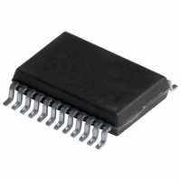
74ABT652ADB,112 NXP Semiconductors, 74ABT652ADB,112 Datasheet - Page 6

74ABT652ADB,112
Manufacturer Part Number
74ABT652ADB,112
Description
IC TRANSCVR 8BIT N-INV 24SSOP
Manufacturer
NXP Semiconductors
Series
74ABTr
Datasheet
1.74ABT652APW118.pdf
(19 pages)
Specifications of 74ABT652ADB,112
Logic Type
Transceiver, Inverting
Package / Case
24-SSOP
Number Of Elements
1
Number Of Bits Per Element
8
Current - Output High, Low
32mA, 64mA
Voltage - Supply
4.5 V ~ 5.5 V
Operating Temperature
-40°C ~ 85°C
Mounting Type
Surface Mount
Logic Family
74ABT
Number Of Channels Per Chip
8
Input Level
TTL
Output Level
TTL
Output Type
3-State
High Level Output Current
- 32 mA
Low Level Output Current
64 mA
Propagation Delay Time
5.1 ns
Supply Voltage (max)
5.5 V
Supply Voltage (min)
4.5 V
Maximum Operating Temperature
+ 85 C
Function
Transceiver/Register
Input Bias Current (max)
30000 uA
Minimum Operating Temperature
- 40 C
Mounting Style
SMD/SMT
Polarity
Non-Inverting
Number Of Circuits
8
Lead Free Status / RoHS Status
Lead free / RoHS Compliant
Lead Free Status / RoHS Status
Lead free / RoHS Compliant, Lead free / RoHS Compliant
Other names
74ABT652ADB
74ABT652ADB
935192700112
74ABT652ADB
935192700112
NXP Semiconductors
6. Functional description
Table 3.
[1]
[2]
[3]
74ABT652A_2
Product data sheet
Inputs
OEAB
L
L
X
H
L
L
L
L
H
H
H
H = HIGH voltage level;
L = LOW voltage level;
X = don’t care;
The data output function may be enabled or disabled by various signals at the OEBA and OEAB inputs. Data input functions are always
enabled, i.e., data at the bus pins will be stored on every LOW-to-HIGH transition of the clock.
If both select controls (SAB and SBA) are LOW, then clocks can occur simultaneously. If either select control is HIGH, the clocks must
be staggered in order to load both registers.
= LOW-to-HIGH clock transition.
OEBA
H
H
H
H
X
L
L
L
H
H
L
Function table
6.1 Function table
CPAB
H or L
H or L
X
X
X
H or L
H or L
Figure 3
performed with the 74ABT652A.
The select pins determine whether data is stored or transferred through the device in real
time.
The output enable pins determine the direction of the data flow.
[1]
CPBA
H or L
H or L
X
H or L
X
X
H or L
demonstrates the four fundamental bus-management functions that can be
All information provided in this document is subject to legal disclaimers.
SAB
X
X
X
[3]
X
X
X
X
L
H
H
Rev. 02 — 12 March 2010
SBA
X
X
X
X
X
[3]
L
H
X
X
H
Data I/O
An
input
input
input
input
unspecified
output
unspecified
output
output
output
input
input
output
Octal transceiver/register; non-inverting; 3-state
[2]
[2]
Bn
input
input
unspecified
output
unspecified
output
input
input
input
input
output
output
output
[2]
[2]
74ABT652A
Operating mode
isolation
store A and B data
store A, hold B
store A in both registers
hold A, store B
store B in both registers
real time B data to A bus
stored B data to A bus
real time A data to B bus
store A data to B bus
stored A data to B bus;
stored B data to A bus
© NXP B.V. 2010. All rights reserved.
6 of 19


