IDT74LVC16244APAG IDT, Integrated Device Technology Inc, IDT74LVC16244APAG Datasheet - Page 5
IDT74LVC16244APAG
Manufacturer Part Number
IDT74LVC16244APAG
Description
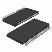
IC BUFF DVR TRI-ST 16BIT 48TSSOP
Manufacturer
IDT, Integrated Device Technology Inc
Series
74LVCr
Datasheet
1.IDT74LVC16244APAG8.pdf
(6 pages)
Specifications of IDT74LVC16244APAG
Logic Type
Buffer/Line Driver, Non-Inverting
Number Of Elements
4
Number Of Bits Per Element
4
Current - Output High, Low
24mA, 24mA
Voltage - Supply
2.7 V ~ 3.6 V
Operating Temperature
-40°C ~ 85°C
Mounting Type
Surface Mount
Package / Case
48-TSSOP
Logic Family
LVC
Logical Function
Buffer/Line Driver
Number Of Elements
4
Number Of Channels
16
Number Of Inputs
16
Number Of Outputs
16
Operating Supply Voltage (typ)
3.3V
Output Type
3-State
Polarity
Non-Inverting
Propagation Delay Time
6.2ns
High Level Output Current
-24mA
Low Level Output Current
24mA
Operating Supply Voltage (max)
3.6V
Operating Supply Voltage (min)
2.7V
Quiescent Current
10uA
Technology
CMOS
Pin Count
48
Mounting
Surface Mount
Operating Temp Range
-40C to 85C
Operating Temperature Classification
Industrial
Lead Free Status / RoHS Status
Lead free / RoHS Compliant
Lead Free Status / RoHS Status
Compliant, Lead free / RoHS Compliant
Other names
74LVC16244APAG
Available stocks
Company
Part Number
Manufacturer
Quantity
Price

Part Number:
IDT74LVC16244APAG
Manufacturer:
IDT
Quantity:
20 000


TEST CIRCUITS AND WAVEFORMS
TEST CONDITIONS
NOTES:
1. Pulse Generator for All Pulses: Rate ≤ 10MHz; t
2. Pulse Generator for All Pulses: Rate ≤ 10MHz; t
SWITCH POSITION
NOTES:
1.
2.
DEFINITIONS:
C
R
IDT74LVC16244A
3.3V CMOS 16-BIT BUFFER/DRIVER WITH 3-STATE OUTPUTS
L
T
Symbol
Generator
V
= Termination resistance: should be equal to Z
= Load capacitance: includes jig and probe capacitance.
V
V
For t
For t
LOAD
V
V
C
Pulse
HZ
LZ
IH
T
L
OUTPUT 2
OUTPUT 1
SK
SK
(b) OUTPUT1 and OUTPUT2 are in the same bank.
(o) OUTPUT1 and OUTPUT2 are any two outputs.
All Other Tests
(1, 2)
Disable High
INPUT
Disable Low
Enable High
Enable Low
Open Drain
V
CC
Test
(1)
= 3.3V±0.3V V
V
300
300
2.7
1.5
50
6
IN
Test Circuit for All Outputs
t
SK
(x)
Output Skew - t
R
= t
T
t
D.U.T.
PLH1
V
PLH2
CC
CC
t
PLH2
(1)
300
300
2.7
1.5
50
6
-
t
= 2.7V
SK
t
PLH1
V
(x)
OUT
OUT
SK
F
F
or
t
(
≤ 2ns; t
≤ 2.5ns; t
PHL1
X
V
of the Pulse Generator.
t
)
CC
C
PHL2
t
PHL2
L
(2)
2 x Vcc
Switch
Vcc / 2
= 2.5V±0.2V
R
V
t
GND
Open
-
SK
Vcc
150
150
LOAD
30
R
≤ 2ns.
t
PHL1
500Ω
500Ω
≤ 2.5ns.
(x)
LVC Link
LVC Link
V
V
0V
V
V
V
V
V
V
IH
T
OH
T
OL
OH
T
OL
V
Open
GND
Unit
LOAD
mV
mV
pF
V
V
V
5
NOTE:
1. Diagram shown for input Control Enable-LOW and input Control Disable-HIGH.
ASYNCHRONOUS
SYNCHRONOUS
INPUT TRANSITION
INPUT TRANSITION
OPPOSITE PHASE
NORMALLY
NORMALLY
HIGH-LOW-HIGH
CONTROL
CONTROL
LOW-HIGH-LOW
CONTROL
SAME PHASE
OUTPUT
OUTPUT
TIMING
INPUT
INPUT
DATA
INPUT
HIGH
OUTPUT
LOW
Set-up, Hold, and Release Times
PULSE
PULSE
Enable and Disable Times
CLOSED
SWITCH
SWITCH
ENABLE
OPEN
Propagation Delay
t
t
PZH
PZL
Pulse Width
t
t
PLH
PLH
INDUSTRIAL TEMPERATURE RANGE
t
SU
t
SU
V
V
0V
V
T
T
LOAD/2
t
W
t
REM
t
H
t
PHZ
t
t
DISABLE
PHL
PHL
t
H
t
PLZ
LVC Link
LVC Link
V
V
LVC Link
T
T
LVC Link
V
V
0V
V
V
V
V
V
0V
V
V
0V
V
V
V
V
V
0V
OH
IH
T
T
OL
IH
T
IH
T
LOAD/2
OL+
OL
OH
OH-
V
V
0V
V
V
0V
V
V
0V
V
V
0V
IH
T
IH
T
IH
T
IH
T
V
V
HZ
LZ
Related parts for IDT74LVC16244APAG
Image
Part Number
Description
Manufacturer
Datasheet
Request
R

Part Number:
Description:
TRANSLATION DEVICE DPI 80-PQFP
Manufacturer:
IDT, Integrated Device Technology Inc
Datasheet:
Part Number:
Description:
IDT PART
Manufacturer:
IDT, Integrated Device Technology Inc
Datasheet:
Part Number:
Description:
IC LIU T1/E1/J1 OCTAL 256PBGA
Manufacturer:
IDT, Integrated Device Technology Inc
Datasheet:

Part Number:
Description:
IC FREQ TIMING GENERATOR 28TSSOP
Manufacturer:
IDT, Integrated Device Technology Inc
Datasheet:
Part Number:
Description:
IC CLK DVR PLL 1:10 40VFQFPN
Manufacturer:
IDT, Integrated Device Technology Inc
Datasheet:
Part Number:
Description:
IC CLK FANOUT BUFFER 1:18 32LQFP
Manufacturer:
IDT, Integrated Device Technology Inc
Datasheet:
Part Number:
Description:
IC CLK FANOUT BUFFER 1:18 32LQFP
Manufacturer:
IDT, Integrated Device Technology Inc
Datasheet:
Part Number:
Description:
IC CK505 VREG/RES 56TSSOP
Manufacturer:
IDT, Integrated Device Technology Inc
Datasheet:

Part Number:
Description:
IC SDRAM CLK DVR 1:10 48-TSSOP
Manufacturer:
IDT, Integrated Device Technology Inc
Datasheet:

Part Number:
Description:
IC CLK DVR PLL 1:10 48TSSOP
Manufacturer:
IDT, Integrated Device Technology Inc
Datasheet:
Part Number:
Description:
IC FLEXPC CLK PROGR P4 56-TSSOP
Manufacturer:
IDT, Integrated Device Technology Inc
Datasheet:
Part Number:
Description:
IC FLEXPC CLK PROGR P4 56-TSSOP
Manufacturer:
IDT, Integrated Device Technology Inc
Datasheet:
Part Number:
Description:
IC FLEXPC CLK PROGR P4 56-SSOP
Manufacturer:
IDT, Integrated Device Technology Inc
Datasheet:

Part Number:
Description:
IC PLL CLK DRIVER 2.5V 28-TSSOP
Manufacturer:
IDT, Integrated Device Technology Inc
Datasheet:
Part Number:
Description:
IC CLOCK DRIVER 2.5V 24-TSSOP
Manufacturer:
IDT, Integrated Device Technology Inc
Datasheet: