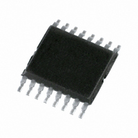
74LVC163PW,118 NXP Semiconductors, 74LVC163PW,118 Datasheet - Page 2

74LVC163PW,118
Manufacturer Part Number
74LVC163PW,118
Description
IC 4-BIT SYNC BIN CNTR 16TSSOP
Manufacturer
NXP Semiconductors
Series
74LVCr
Datasheet
1.74LVC163PW118.pdf
(21 pages)
Specifications of 74LVC163PW,118
Package / Case
16-TSSOP
Logic Type
Binary Counter
Direction
Up
Number Of Elements
1
Number Of Bits Per Element
4
Reset
Synchronous
Timing
Synchronous
Count Rate
150MHz
Trigger Type
Positive Edge
Voltage - Supply
1.2 V ~ 3.6 V
Operating Temperature
-40°C ~ 125°C
Mounting Type
Surface Mount
Logic Family
74LVC
Number Of Bits
4
Operating Supply Voltage
1 V to 3.6 V
Operating Temperature Range
- 40 C to + 125 C
Mounting Style
SMD/SMT
Lead Free Status / RoHS Status
Lead free / RoHS Compliant
Lead Free Status / RoHS Status
Lead free / RoHS Compliant, Lead free / RoHS Compliant
Other names
568-2293-2
74LVC163PW-T
935210560118
74LVC163PW-T
935210560118
Philips Semiconductors
FEATURES
DESCRIPTION
The 74LVC163 is a high-performance, low-power,
low-voltage, Si-gate CMOS device and superior to most
advanced CMOS compatible TTL families.
The 74LVC163 is a synchronous presettable binary
counter which features an internal look-head carry and can
be used for high-speed counting. Synchronous operation
is provided by having all flip-flops clocked simultaneously
on the positive-going edge of the clock (pin CP). The
outputs (pins Q0 to Q3) of the counters may be preset to a
2004 May 05
Wide supply voltage range from 1.2 V to 3.6 V
Complies with JEDEC standard JESD8-B/JESD36
Inputs accept voltages up to 5.5 V
CMOS low power consumption
Direct interface with TTL levels
Synchronous reset
Synchronous counting and loading
Two count enable inputs for n-bit cascading
Positive edge-triggered clock.
ESD protection:
– HBM EIA/JESD22-A114-B exceeds 2000 V
– MM EIA/JESD22-A115-A exceeds 200 V.
Specified from 40 C to +85 C and 40 C to +125 C.
Presettable synchronous 4-bit binary
counter; synchronous reset
2
HIGH-level or LOW-level. A LOW-level at the parallel
enable input (pin PE) disables the counting action and
causes the data at the data inputs (pins D0 to D3) to be
loaded into the counter on the positive-going edge of the
clock (provided that the set-up and hold time requirements
for PE are met). Preset takes place regardless of the levels
at count enable inputs (pins CEP and CET). A LOW-level
at the master reset input (pin MR) sets all four outputs of
the flip-flops (pins Q0 to Q3) to LOW-level after the next
positive-going transition on the clock input (pin CP)
(provided that the set-up and hold time requirements for
PE are met). This action occurs regardless of the levels at
input pins PE, CET and CEP. This synchronous reset
feature enables the designer to modify the maximum count
with only one external NAND gate.
The look-ahead carry simplifies serial cascading of the
counters. Both count enable inputs (pins CEP and CET)
must be HIGH to count. The CET input is fed forward to
enable the terminal count output (pin TC). The TC output
thus enabled will produce a HIGH output pulse of a
duration approximately equal to a HIGH-level output of Q0.
This pulse can be used to enable the next cascaded stage.
The maximum clock frequency for the cascaded counters
is determined by t
(set-up time CEP to CP) according to the
formula:
f
max
=
------------------------------------ -
t
PHL max
PHL
(propagation delay CP to TC) and t
1
+
t
su
.
Product specification
74LVC163
su


