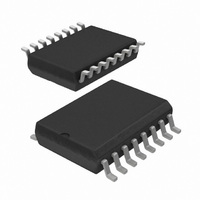
74HCT7403D,518 NXP Semiconductors, 74HCT7403D,518 Datasheet - Page 24

74HCT7403D,518
Manufacturer Part Number
74HCT7403D,518
Description
IC FIFO REGISTER 64X4 3ST 16SOIC
Manufacturer
NXP Semiconductors
Series
74HCTr
Datasheet
1.74HCT7403N112.pdf
(28 pages)
Specifications of 74HCT7403D,518
Function
Asynchronous, Synchronous
Memory Size
256 (64 x 4)
Data Rate
15MHz
Voltage - Supply
4.5 V ~ 5.5 V
Mounting Type
Surface Mount
Package / Case
16-SOIC (0.300", 7.5mm Width)
Lead Free Status / RoHS Status
Lead free / RoHS Compliant
Operating Temperature
-
Access Time
-
Other names
74HCT7403D-T
74HCT7403D-T
933999390518
74HCT7403D-T
933999390518
Philips Semiconductors
Expanded format
Figure 20 shows two cascaded FIFOs
providing a capacity of 128 words x
4 bits. Figure 21 shows the signals on
the nodes of both FIFOs after the
application of a SI pulse, when both
FIFOs are initially empty. After a
ripple through delay, data arrives at
the output of FIFO
being HIGH, a DOR
generated. The requirements of SI
Note to Fig.20
The “7403” is easily cascaded to increase word capacity without any external circuitry. In cascaded format, all necessary
communications are handled by the FIFOs. Figures 21 and 22 demonstrate the intercommunication timing between
FIFO
shifted empty again.
September 1993
4-Bit x 64-word FIFO register; 3-state
A
and FIFO
B
DATA INPUT
. Figure 23 provides an overview of pulses and timing of two cascaded FIFOs, when shifted full and
A
. Due to SO
A
pulse is
DIR
MR
OE
SI
Fig.20 Cascading for increased word capacity; 128 words x 4 bits.
4
A
B
SI
DIR
D nA
A
A
MR
and D
pulse width and the timing between
the rising edge of DOR
After a second ripple through delay,
data arrives at the output of FIFO
Figure 22 shows the signals on the
nodes of both FIFOs after the
application of a SO
FIFOs are initially full. After a
bubble-up delay a DIR
generated, which acts as a SO
FIFO A
7403
nB
OE
DOR A
are satisfied by the DOR
SO A
Q nA
4
24
B
pulse, when both
DIR
B
SI
D nB
A
pulse is
B
and Q
MR
B
FIFO B
7403
A
nA
pulse
.
OE
A
B
DOR B
.
Q nB
SO B
MGA679
for FIFO
from the output of FIFO
of FIFO
SO
the pulse width of DOR
second bubble-up delay an empty
space arrives at D
DIR
the waveforms at all external nodes of
both FIFOs during a complete shift-in
and shift-out sequence.
4
A
A
pulse for FIFO
goes HIGH. Figure 23 shows
DOR
SO
DATA OUTPUT
B
A
. The requirements of the
. One word is transferred
74HC/HCT7403
Product specification
nA
A
, at which time
is satisfied by
B
A
. After a
to the input


