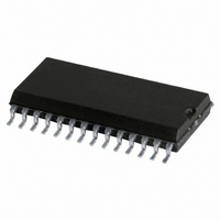
74HCT7030D,118 NXP Semiconductors, 74HCT7030D,118 Datasheet - Page 21

74HCT7030D,118
Manufacturer Part Number
74HCT7030D,118
Description
IC 9X64 FIFO REGISTER 3ST 28SOIC
Manufacturer
NXP Semiconductors
Series
74HCTr
Datasheet
1.74HCT7030D118.pdf
(22 pages)
Specifications of 74HCT7030D,118
Function
Asynchronous, Synchronous
Memory Size
576 (9 x 64)
Data Rate
33MHz
Voltage - Supply
4.5 V ~ 5.5 V
Mounting Type
Surface Mount
Package / Case
28-SOIC (7.5mm Width)
Lead Free Status / RoHS Status
Lead free / RoHS Compliant
Operating Temperature
-
Access Time
-
Other names
74HCT7030D-T
74HCT7030D-T
933798900118
74HCT7030D-T
933798900118
Philips Semiconductors
December 1990
9-bit x 64-word FIFO register; 3-state
Sequence 1 (Both FIFOs empty, starting shift-in process):
After a MR pulse has been applied FIFO
LOW due to no valid data being present at the outputs. The DIR flags are set HIGH due to the FIFOs being
ready to accept data. SO
words to ripple through to the output stage of FIFO
at the output of FIFO
a second bit ripples through to the output after which DOR
Sequence 2 (FIFO
After the MR pulse, a series of 64 SI pulses are applied. When 64 words are shifted in, DIR
due to FIFO
Sequence 3 (FIFO
When 65 words are shifted in, DOR
Q
and both FIFOs are full (7). Additional pulses have no effect.
Sequence 4 (Both FIFOs full, starting shift-out process):
SI
empty locations to bubble-up to the input stage of FIFO
location arrives at the input of FIFO
SI
DIR
Sequence 5 (FIFO
At the start of sequence 5 FIFO
being shifted in in sequence 4. An additional series of SO
words from FIFO
Sequence 6 (FIFO
After the next SO
another 63 SO
have no effect. The last word remains available at the output Q
nA
A
A
is held HIGH and two SO
is made LOW and now the second empty location reaches the input stage of FIFO
A
Fig.22 Waveforms showing the functionality and intercommunication between two FIFOs (refer to Fig.19).
remains HIGH, being the polarity of the 65th data word (6). After the 128th SI pulse, DIR remains LOW
remains HIGH (11).
B
being full (5). DOR
B
pulses, DOR
A
B
B
A
A
are shifted into FIFO
B
pulse, DIR
runs full):
runs full):
runs empty):
runs empty):
B
, a DOR
B
is held HIGH and two SI
B
B
B
B
pulses are applied (8). These pulses shift out two words and thus allow two
remains LOW due to both FIFOs being empty (14). Additional SO
A
remains HIGH due to the input stage of FIFO
pulse is generated (3). When SO
A
contains 63 valid words due to two words being shifted out and one word
goes LOW due to FIFO
A
A
, a DIR
remains HIGH due to valid data remaining at the output of FIFO
B
A
. DOR
and FIFO
A
pulse is generated (10) and a new word is shifted into FIFO
A
remains LOW (12).
A
A
B
and to the input stage of FIFO
pulses are applied (1). These pulses allow two data
are empty. The DOR flags of FIFO
B
, and proceed to FIFO
B
A
B
pulses are applied. After 63 SO
being empty.
goes HIGH (4).
n
.
B
goes LOW, the first bit is shifted out and
21
B
being empty (13). After
A
(9). When the first empty
B
(2). When data arrives
A
, after which
A
and FIFO
B
B
remains LOW
pulses, all
B
pulses
B
A
go
.
A
.
74HC/HCT7030
Product specification


