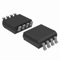
74LVC1G74DC,125 NXP Semiconductors, 74LVC1G74DC,125 Datasheet - Page 17

74LVC1G74DC,125
Manufacturer Part Number
74LVC1G74DC,125
Description
IC SNGL D FF POS-EDG TRIG 8VSSOP
Manufacturer
NXP Semiconductors
Series
74LVCr
Type
D-Typer
Datasheet
1.74LVC1G74DC125.pdf
(25 pages)
Specifications of 74LVC1G74DC,125
Output Type
Differential
Package / Case
US8, 8-VSSOP
Function
Set(Preset) and Reset
Number Of Elements
1
Number Of Bits Per Element
1
Frequency - Clock
200MHz
Trigger Type
Positive Edge
Current - Output High, Low
32mA, 32mA
Voltage - Supply
1.65 V ~ 5.5 V
Operating Temperature
-40°C ~ 125°C
Mounting Type
Surface Mount
Number Of Circuits
1
Logic Family
74LVC
Logic Type
CMOS
Polarity
Inverting/Non-Inverting
Input Type
Single-Ended
Propagation Delay Time
13.4 ns
High Level Output Current
- 32 mA
Low Level Output Current
32 mA
Supply Voltage (max)
5.5 V
Maximum Operating Temperature
+ 125 C
Mounting Style
SMD/SMT
Minimum Operating Temperature
- 40 C
Supply Voltage (min)
1.65 V
Technology
CMOS
Number Of Bits
1
Number Of Elements
1
Clock-edge Trigger Type
Positive-Edge
Operating Supply Voltage (typ)
1.8/2.5/3.3/5V
Package Type
VSSOP
Operating Supply Voltage (min)
1.65V
Operating Supply Voltage (max)
5.5V
Operating Temp Range
-40C to 125C
Operating Temperature Classification
Automotive
Mounting
Surface Mount
Pin Count
8
Lead Free Status / RoHS Status
Lead free / RoHS Compliant
Delay Time - Propagation
-
Lead Free Status / Rohs Status
Lead free / RoHS Compliant
Other names
568-4494-2
74LVC1G74DC-G
74LVC1G74DC-G
935274973125
74LVC1G74DC-G
74LVC1G74DC-G
935274973125
NXP Semiconductors
Fig 14. Package outline SOT1089 (XSON8)
74LVC1G74
Product data sheet
XSON8: extremely thin small outline package; no leads;
8 terminals; body 1.35 x 1 x 0.5 mm
Dimensions
Note
1. Including plating thickness.
2. Visible depending upon used manufacturing technology.
mm
SOT1089
Unit
Outline
version
max
nom
min
A
0.5
(1)
0.04
A
terminal 1
index area
terminal 1
index area
1
0.20
0.15
0.12
(4×)
b
IEC
b
(2)
1.40
1.35
1.30
4
1
D
1.05
1.00
0.95
E
L
1
0.55 0.35
MO-252
JEDEC
e
All information provided in this document is subject to legal disclaimers.
E
e
e
1
References
L
0
Single D-type flip-flop with set and reset; positive edge trigger
0.35
0.30
0.27
Rev. 9 — 5 August 2010
L
5
8
0.40
0.35
0.32
L
1
e
JEITA
D
1
scale
0.5
A
1 mm
(8×)
A
1
(2)
detail X
European
projection
X
74LVC1G74
© NXP B.V. 2010. All rights reserved.
Issue date
10-04-09
10-04-12
sot1089_po
SOT1089
17 of 25


