N74F74N,602 NXP Semiconductors, N74F74N,602 Datasheet - Page 5
N74F74N,602
Manufacturer Part Number
N74F74N,602
Description
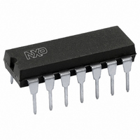
IC FLIP FLOP DUAL D TYPE 14DIP
Manufacturer
NXP Semiconductors
Series
74Fr
Type
D-Typer
Datasheet
1.N74F74N602.pdf
(8 pages)
Specifications of N74F74N,602
Output Type
Differential
Package / Case
14-DIP (0.300", 7.62mm)
Function
Set(Preset) and Reset
Number Of Elements
2
Number Of Bits Per Element
1
Frequency - Clock
125MHz
Trigger Type
Positive Edge
Current - Output High, Low
1mA, 20mA
Voltage - Supply
4.5 V ~ 5.5 V
Operating Temperature
-40°C ~ 85°C
Mounting Type
Through Hole
Number Of Circuits
2
Logic Family
F
Logic Type
D-Type Edge Triggered Flip-Flop
Polarity
Inverting/Non-Inverting
Input Type
Single-Ended
Propagation Delay Time
6.2 ns
High Level Output Current
- 1 mA
Low Level Output Current
20 mA
Supply Voltage (max)
5.5 V
Maximum Operating Temperature
+ 70 C
Mounting Style
Through Hole
Minimum Operating Temperature
0 C
Supply Voltage (min)
4.5 V
Technology
Bipolar
Number Of Bits
2
Number Of Elements
2
Clock-edge Trigger Type
Positive-Edge
Operating Supply Voltage (typ)
5V
Package Type
DIP
Frequency (max)
125MHz
Operating Supply Voltage (min)
4.5V
Operating Supply Voltage (max)
5.5V
Operating Temp Range
0C to 70C
Operating Temperature Classification
Commercial
Mounting
Through Hole
Pin Count
14
Lead Free Status / RoHS Status
Lead free / RoHS Compliant
Delay Time - Propagation
-
Lead Free Status / Rohs Status
Compliant
Other names
568-1734-5
933668140602
N74F74N
933668140602
N74F74N


Philips Semiconductors
AC WAVEFORMS
For all waveforms, V
The shaded areas indicate when the input is permitted to
change for predictable output performance.
Waveform 1. Propagation delay for data to output, data setup
time and hold times, and clock width, and maximum clock
frequency
Waveform 3. Recovery time for set or reset to clock
TEST CIRCUIT AND WAVEFORMS
1996 Mar 12
CPn
Dn
Qn
Qn
SDn or RDn
Dual D-type flip-flop
DEFINITIONS:
R
C
R
T
L
L
GENERATOR
= Load resistor;
= Load capacitance includes jig and probe capacitance;
= Termination resistance should be equal to Z
CPn
PULSE
see AC ELECTRICAL CHARACTERISTICS for value.
see AC ELECTRICAL CHARACTERISTICS for value.
pulse generators.
t
V
su
V
M
Test Circuit for Totem-Pole Outputs
M
(L)
t
h
M
V
V
(L)
t
t
PLH
PHL
IN
M
= 1.5V.
t
w
(H)
R
T
V
V
V
D.U.T.
M
1/f
V
M
M
CC
max
V
OUT
t
w
V
(L)
M
t
rec
t
V
su
M
C
(H)
L
R
t
L
h
V
V
OUT
(H)
t
M
V
t
PHL
M
PLH
M
V
V
M
M
SF00051
of
SF01276
NEGATIVE
PULSE
POSITIVE
PULSE
family
5
74F
Waveform 2. Propagation delay for set and reset to output,
set and reset pulse width
SDn
RDn
Qn
Qn
90%
10%
V
amplitude
M
3.0V
V
INPUT PULSE REQUIREMENTS
V
M
90%
M
t
t
10%
PLH
PHL
t
w
t
t
TLH (
THL (
Input Pulse Definition
(L)
1.5V
V
M
t
t
r
f
)
)
V
V
rep. rate
M
M
1MHz
t
t
w
w
V
M
t
t
TLH (
THL (
500ns
t
t
r
V
f
t
10%
90%
)
)
w
M
V
V
M
M
2.5ns
t
TLH
t
PHL
t
PLH
Product specification
t
V
w
V
90%
10%
M
M
(L)
2.5ns
t
THL
74F74
AMP (V)
0V
0V
AMP (V)
SF00050
SF00006
V
M
Related parts for N74F74N,602
Image
Part Number
Description
Manufacturer
Datasheet
Request
R

Part Number:
Description:
NXP Semiconductors designed the LPC2420/2460 microcontroller around a 16-bit/32-bitARM7TDMI-S CPU core with real-time debug interfaces that include both JTAG andembedded trace
Manufacturer:
NXP Semiconductors
Datasheet:

Part Number:
Description:
NXP Semiconductors designed the LPC2458 microcontroller around a 16-bit/32-bitARM7TDMI-S CPU core with real-time debug interfaces that include both JTAG andembedded trace
Manufacturer:
NXP Semiconductors
Datasheet:
Part Number:
Description:
NXP Semiconductors designed the LPC2468 microcontroller around a 16-bit/32-bitARM7TDMI-S CPU core with real-time debug interfaces that include both JTAG andembedded trace
Manufacturer:
NXP Semiconductors
Datasheet:
Part Number:
Description:
NXP Semiconductors designed the LPC2470 microcontroller, powered by theARM7TDMI-S core, to be a highly integrated microcontroller for a wide range ofapplications that require advanced communications and high quality graphic displays
Manufacturer:
NXP Semiconductors
Datasheet:
Part Number:
Description:
NXP Semiconductors designed the LPC2478 microcontroller, powered by theARM7TDMI-S core, to be a highly integrated microcontroller for a wide range ofapplications that require advanced communications and high quality graphic displays
Manufacturer:
NXP Semiconductors
Datasheet:
Part Number:
Description:
The Philips Semiconductors XA (eXtended Architecture) family of 16-bit single-chip microcontrollers is powerful enough to easily handle the requirements of high performance embedded applications, yet inexpensive enough to compete in the market for hi
Manufacturer:
NXP Semiconductors
Datasheet:
Part Number:
Description:
The XA-S3 device is a member of Philips Semiconductors? XA(eXtended Architecture) family of high performance 16-bitsingle-chip microcontrollers
Manufacturer:
NXP Semiconductors
Datasheet:

Part Number:
Description:
The NXP BlueStreak LH75401/LH75411 family consists of two low-cost 16/32-bit System-on-Chip (SoC) devices
Manufacturer:
NXP Semiconductors
Datasheet:
Part Number:
Description:
The NXP LPC3130/3131 combine an 180 MHz ARM926EJ-S CPU core, high-speed USB2
Manufacturer:
NXP Semiconductors
Datasheet:
Part Number:
Description:
The NXP LPC3141 combine a 270 MHz ARM926EJ-S CPU core, High-speed USB 2
Manufacturer:
NXP Semiconductors
Part Number:
Description:
The NXP LPC3143 combine a 270 MHz ARM926EJ-S CPU core, High-speed USB 2
Manufacturer:
NXP Semiconductors

Part Number:
Description:
The NXP LPC3152 combines an 180 MHz ARM926EJ-S CPU core, High-speed USB 2
Manufacturer:
NXP Semiconductors
Part Number:
Description:
The NXP LPC3154 combines an 180 MHz ARM926EJ-S CPU core, High-speed USB 2
Manufacturer:
NXP Semiconductors

Part Number:
Description:
Standard level N-channel enhancement mode Field-Effect Transistor (FET) in a plastic package using NXP High-Performance Automotive (HPA) TrenchMOS technology
Manufacturer:
NXP Semiconductors
Datasheet: