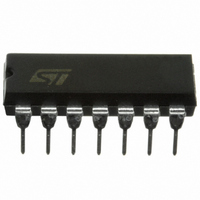
M74HCT74B1R STMicroelectronics, M74HCT74B1R Datasheet - Page 3

M74HCT74B1R
Manufacturer Part Number
M74HCT74B1R
Description
IC FLIP/FLOP DUAL D TYPE 14-DIP
Manufacturer
STMicroelectronics
Series
74HCTr
Type
D-Typer
Datasheet
1.M74HCT74RM13TR.pdf
(10 pages)
Specifications of M74HCT74B1R
Function
Set(Preset) and Reset
Output Type
Differential
Number Of Elements
2
Number Of Bits Per Element
1
Frequency - Clock
48MHz
Delay Time - Propagation
21ns
Trigger Type
Positive Edge
Current - Output High, Low
4mA, 4mA
Voltage - Supply
4.5 V ~ 5.5 V
Operating Temperature
-55°C ~ 125°C
Mounting Type
Through Hole
Package / Case
14-DIP (0.300", 7.62mm)
Logic Family
HCT
Technology
CMOS
Number Of Bits
2
Number Of Elements
2
Clock-edge Trigger Type
Positive-Edge
Polarity
Invert/Non-Invert
Operating Supply Voltage (typ)
5V
Package Type
PDIP
Propagation Delay Time
50ns
Low Level Output Current
4mA
High Level Output Current
-4mA
Frequency (max)
18MHz
Operating Supply Voltage (min)
4.5V
Operating Supply Voltage (max)
5.5V
Operating Temp Range
-55C to 125C
Operating Temperature Classification
Military
Mounting
Through Hole
Pin Count
14
Number Of Circuits
2
Logic Type
D-Type Flip-Flop
Input Type
Single-Ended
Supply Voltage (max)
5.5 V
Maximum Operating Temperature
+ 125 C
Mounting Style
Through Hole
Minimum Operating Temperature
- 55 C
Supply Voltage (min)
4.5 V
Lead Free Status / RoHS Status
Lead free / RoHS Compliant
Other names
497-1922-5
ABSOLUTE MAXIMUM RATINGS
Absolute Maximum Ratings are those values beyond which damage to the device may occur. Functional operation under these conditions is
not implied
(*) 500mW at 65 C; derate to 300mW by 10mW/ C from 65 C to 85 C
RECOMMENDED OPERATING CONDITIONS
DC SPECIFICATIONS
I
CC
Symbol
Symbol
Symbol
V
V
V
V
I
V
V
CC
T
t
I
or I
T
OH
I
V
P
V
OL
I
I
T
r
IH
V
OK
I
V
CC
IL
I
stg
, t
CC
IK
O
CC
op
O
D
O
L
I
I
f
GND
High Level Input
Voltage
Low Level Input
Voltage
High Level Output
Voltage
Low Level Output
Voltage
Input Leakage
Current
Quiescent Supply
Current
Additional Worst
Case Supply
Current
Supply Voltage
DC Input Voltage
DC Output Voltage
DC Input Diode Current
DC Output Diode Current
DC Output Current
DC V
Power Dissipation
Storage Temperature
Lead Temperature (10 sec)
Supply Voltage
Input Voltage
Output Voltage
Operating Temperature
Input Rise and Fall Time (V
Parameter
CC
or Ground Current
V
(V)
4.5
5.5
4.5
5.5
4.5
4.5
5.5
5.5
5.5
to
to
CC
Test Condition
Parameter
Parameter
CC
V
V
Other Inputs at
I
I
Per Input pin
= V
= V
V
I
V
= 4.5 to 5.5V)
I
I
O
I
O
V
O
CC
I
O
=-4.0 mA
=4.0 mA
I
=-20 A
= 0.5V or
=20 A
I
CC
CC
= 2.4V
O
or GND
= 0
or GND
or GND
Min.
4.18
2.0
4.4
T
A
Typ.
4.31
0.17
= 25°C
4.5
0.0
Max.
0.26
0.8
0.1
2.0
0.1
2
Value
-40 to 85°C
Min.
4.13
2.0
4.4
-0.5 to V
-0.5 to V
-65 to +150
-55 to 125
-0.5 to +7
4.5 to 5.5
0 to V
0 to V
0 to 500
Max.
0.33
500(*)
Value
Value
0.8
0.1
2.9
20
300
1
20
20
25
50
CC
CC
CC
CC
-55 to 125°C
+ 0.5
+ 0.5
Min.
4.10
2.0
4.4
M74HCT74
Max.
0.40
0.8
0.1
3.0
40
1
Unit
Unit
mW
mA
mA
mA
mA
°C
°C
°C
ns
Unit
V
V
V
V
V
V
mA
V
V
V
V
3/10
A
A


