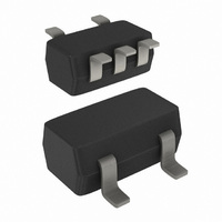
74LVC1G79GW,125 NXP Semiconductors, 74LVC1G79GW,125 Datasheet - Page 10

74LVC1G79GW,125
Manufacturer Part Number
74LVC1G79GW,125
Description
IC SGL D FF POS-EDG TRIG 5-TSSOP
Manufacturer
NXP Semiconductors
Series
74LVCr
Type
D-Typer
Datasheet
1.74LVC1G79GW125.pdf
(20 pages)
Specifications of 74LVC1G79GW,125
Output Type
Non-Inverted
Package / Case
SC-70-5, SC-88A, SOT-323-5, SOT-353, 5-TSSOP
Function
Standard
Number Of Elements
1
Number Of Bits Per Element
1
Frequency - Clock
500MHz
Delay Time - Propagation
1.7ns
Trigger Type
Positive Edge
Current - Output High, Low
32mA, 32mA
Voltage - Supply
1.65 V ~ 5.5 V
Operating Temperature
-40°C ~ 125°C
Mounting Type
Surface Mount
Number Of Circuits
1
Logic Family
LVC
Logic Type
D-Type Edge Triggered Flip-Flop
Polarity
Non-Inverting
Input Type
Single-Ended
Propagation Delay Time
2.2 ns at 3.3 V
High Level Output Current
- 32 mA
Low Level Output Current
32 mA
Supply Voltage (max)
5.5 V
Maximum Operating Temperature
+ 125 C
Mounting Style
SMD/SMT
Minimum Operating Temperature
- 40 C
Supply Voltage (min)
1.65 V
Technology
CMOS
Number Of Bits
1
Number Of Elements
1
Clock-edge Trigger Type
Positive-Edge
Operating Supply Voltage (typ)
1.8/2.5/3.3/5V
Package Type
SOT
Frequency (max)
200MHz
Operating Supply Voltage (min)
1.65V
Operating Supply Voltage (max)
5.5V
Operating Temp Range
-40C to 125C
Operating Temperature Classification
Automotive
Mounting
Surface Mount
Pin Count
5
Lead Free Status / RoHS Status
Lead free / RoHS Compliant
Lead Free Status / RoHS Status
Lead free / RoHS Compliant, Lead free / RoHS Compliant
Other names
568-4838-2
74LVC1G79GW,125
74LVC1G79GW-G
74LVC1G79GW-G
935268675125
74LVC1G79GW,125
74LVC1G79GW-G
74LVC1G79GW-G
935268675125
Available stocks
Company
Part Number
Manufacturer
Quantity
Price
Company:
Part Number:
74LVC1G79GW,125
Manufacturer:
NXP Semiconductors
Quantity:
7 050
NXP Semiconductors
Table 10.
74LVC1G79
Product data sheet
Supply voltage
V
1.65 V to 1.95 V
2.3 V to 2.7 V
2.7 V
3.0 V to 3.6 V
4.5 V to 5.5 V
Fig 9.
CC
Test data is given in
Definitions for test circuit:
R
C
R
V
Test circuit for measuring switching times
L
L
T
EXT
Test data
= Load resistance.
= Load capacitance including jig and probe capacitance.
= Termination resistance should be equal to the output impedance Z
= External voltage for measuring switching times.
Input
V
V
V
2.7 V
2.7 V
V
I
CC
CC
CC
Table
10.
G
All information provided in this document is subject to legal disclaimers.
t
≤ 2.0 ns
≤ 2.0 ns
≤ 2.5 ns
≤ 2.5 ns
≤ 2.5 ns
r
= t
V
Rev. 8 — 30 September 2010
I
f
R T
DUT
V
CC
Load
C
30 pF
30 pF
50 pF
50 pF
50 pF
V
L
O
Single D-type flip-flop; positive-edge trigger
C L
o
of the pulse generator.
V
mna616
EXT
R L
R L
R
1 kΩ
500 Ω
500 Ω
500 Ω
500 Ω
L
74LVC1G79
© NXP B.V. 2010. All rights reserved.
V
t
open
open
open
open
open
PLH
EXT
, t
PHL
10 of 20


