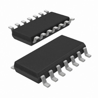
N74F5074D,602 NXP Semiconductors, N74F5074D,602 Datasheet - Page 6

N74F5074D,602
Manufacturer Part Number
N74F5074D,602
Description
IC FLIP FLOP/CLOCK DRIVER 14SOIC
Manufacturer
NXP Semiconductors
Series
74Fr
Type
D-Typer
Datasheet
1.N74F5074D602.pdf
(12 pages)
Specifications of N74F5074D,602
Function
Set(Preset) and Reset
Output Type
Differential
Number Of Elements
2
Number Of Bits Per Element
1
Frequency - Clock
120MHz
Trigger Type
Positive Edge
Current - Output High, Low
15mA, 20mA
Voltage - Supply
4.5 V ~ 5.5 V
Operating Temperature
0°C ~ 70°C
Mounting Type
Surface Mount
Package / Case
14-SOIC (3.9mm Width), 14-SOL
Lead Free Status / RoHS Status
Lead free / RoHS Compliant
Delay Time - Propagation
-
Other names
568-1732-5
935007610602
N74F5074D
935007610602
N74F5074D
1. For conditions shown as MIN or MAX, use the appropriate value specified under recommended operating conditions for the applicable type.
2. All typical values are at V
3. Not more than one output should be shorted at a time. For testing I
4. Measure I
Philips Semiconductors
ABSOLUTE MAXIMUM RATINGS
(Operation beyond the limit set forth in this table may impair the useful life of the device. Unless otherwise noted these limits are over the
operating free air temperature range.)
RECOMMENDED OPERATING CONDITIONS
DC ELECTRICAL CHARACTERISTICS
(Over recommended operating free-air temperature range unless otherwise noted.)
NOTES:
September 14, 1990
V
V
I
V
I
T
T
SYMBOL
V
V
V
I
I
I
T
SYMBOL
IN
OUT
Ik
OH
OL
SYMBOL
V
V
V
I
I
I
I
I
amb
stg
amb
CC
IN
OUT
CC
IH
IL
I
IH
IL
OS
CC
Synchronizing dual D-type flip-flop/clock driver
techniques are preferable in order to minimize internal heating and more accurately reflect operational values. Otherwise, prolonged shorting
of a high output may raise the chip temperature well above normal and thereby cause invalid readings in other parameter tests. In any
sequence of parameter tests, I
OH
OL
IK
Supply voltage
High–level input voltage
Low–level input voltage
Input clamp current
High–level output current
Low–level output current
Operating free air temperature range
CC
Supply voltage
Input voltage
Input current
Voltage applied to output in high output state
Current applied to output in low output state
Operating free air temperature range
Storage temperature range
High–level output voltage
Low–level output voltage
Input clamp voltage
Input current at maximum input voltage
High–level input current
Low–level input current
Short circuit output current
Supply current
with the clock input grounded and all outputs open, then with Q and Q outputs high in turn.
CC
4
PARAMETER
(total)
= 5V, T
OS
tests should be performed last.
amb
PARAMETER
3
CPn, SDn, RDn
= 25 C.
Dn
PARAMETER
V
MAX,
V
V
MAX,
V
V
V
V
V
V
V
V
CC
IH
CC
IH
CC
CC
CC
CC
CC
CC
CC
V
= MIN
= MIN
V
= MIN, V
= MIN, V
= MIN, I
= MAX, V
= MAX, V
= MAX, V
= MAX, V
= MAX
= MAX
CC
CC
OS
6
10%
5%
, the use of high-speed test apparatus and/or sample-and-hold
I
IL
IL
= I
I
I
I
I
= 7.0V
= 2.7V
= 0.5V
= 0.5V
=
=
IK
CONDITIONS
TEST
MIN
4.5
2.0
I
I
0
OH
OL
= MAX
= MAX
1
LIMITS
NOM
5.0
10%V
10%V
5%V
5%V
CC
CC
CC
CC
MAX
–18
–12
–15
5.5
0.8
+70
MIN
–0.5 to +7.0
–65 to +150
20
–0.5 to V
-60
–0.5 to +7.0
2.5
2.7
–30 to +5
RATING
0 to +70
40
LIMITS
TYP
-0.73
0.30
0.30
3.4
20
CC
Product specification
T
A
74F5074
2
= –40 to +85 C
MAX
0.50
0.50
-250
-150
-1.2
100
-20
UNIT
20
30
mA
mA
mA
mA
V
V
V
C
UNIT
mA
mA
UNIT
V
V
V
mA
mA
C
C
V
V
V
V
V
A
A
A
A


