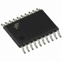
74ACT273MTC Fairchild Semiconductor, 74ACT273MTC Datasheet - Page 3

74ACT273MTC
Manufacturer Part Number
74ACT273MTC
Description
IC FLIP FLOP OCT D TYPE 20-TSSOP
Manufacturer
Fairchild Semiconductor
Series
74ACTr
Type
D-Type Busr
Datasheet
1.74ACT273MTC.pdf
(7 pages)
Specifications of 74ACT273MTC
Function
Master Reset
Output Type
Non-Inverted
Number Of Elements
1
Number Of Bits Per Element
8
Frequency - Clock
189MHz
Delay Time - Propagation
6.5ns
Trigger Type
Positive Edge
Current - Output High, Low
24mA, 24mA
Voltage - Supply
4.5 V ~ 5.5 V
Operating Temperature
-40°C ~ 85°C
Mounting Type
Surface Mount
Package / Case
20-TSSOP
Number Of Circuits
8
Logic Family
74ACT
Logic Type
D-Type Flip-Flop
Polarity
Non-Inverting
Input Type
Single-Ended
Propagation Delay Time
8.5 ns
High Level Output Current
- 24 mA
Low Level Output Current
24 mA
Supply Voltage (max)
5.5 V
Maximum Operating Temperature
+ 85 C
Mounting Style
SMD/SMT
Minimum Operating Temperature
- 40 C
Supply Voltage (min)
4.5 V
Lead Free Status / RoHS Status
Lead free / RoHS Compliant
FM3565 Rev. A.1
The FM3565 block diagram is shown in Figure 1.
Operational Modes
During standard operation, the device will pass data to the Y-Port
either from the I-Port or from one of the internally stored Non-
Volatile Register values.
The I-port values are generated from the motherboard of the
system and may be hardwired or driven by another device. Pull-
up resistors are provided on the device to accommodate this
device being driven by open-drain output drivers. The device
expects standard CMOS input signals. The outputs (Y0-Y4)
operate in the open-drain mode. The OVRD (override) input, when
set to 0, will cause all the outputs to be set to 0. The WP signal, if
set to logic 1, will prevent data from being written to the non-volatile
register.
The functioning of this device is described by the truth table in
Table 1.
The output port is an open-drain output to allow for easy connec-
tion to devices running at different voltage levels. The port is
always active and either passes the value on the I-Port or data
from one of the internal non-volatile registers (SOPRA/B). Chang-
ing the Mux Path is accomplished using the external hardware
controls – OVRD, MUXSEL, and A/B.
The FM3550/60 has 3 registers in total. These registers are made
up of a combination of read-only, write-only and read/write bits.
The two registers are listed below.
Serial Output Port Register A(SOPRA) Address: 00H - A read/
write register that contains the new value of SOPRA.
Serial Output Port Register B(SOPRB) Address: 01H - A read/
write register that contains the new value for SOPRB.
Parallel Input Port Register (PIPR) Address: 02H - A read-only
register that is loaded with the 5-bit value of the I-Port.
(Address 000b and 001b)
b7-b6 - Multiplexer Select Bits (MXSB,MXSA)
00 - Multiplexer passes the SOPR(A).
01 - Multiplexer passer the SOPR(B).
10 - Multiplexer defaults to passing the I-Port Value.
b5, b3-b0 - Data Field. New value to be output through the
multiplexer.
(Address 002b)
b7-b5 - Address field. Value is always 000
b4-b0 - Data Field. Value is equal to the value on the I-Port.
The external Port Register captures the value on the I-Port. Data
is latched into this register on the first clock after a start condition
is seen. This insures that a valid value will always be in this register
if it is read. This register is a-read only register with respect to the
IIC port.
b7
b7
0
0
b6
b6
0
0
b5
b5
I5
0
b4
b4
I4
0
b3
b3
I3
I3
b2
b2
I2
I2
www.fairchildsemi.com
www.fairchildsemi.com
B1
B1
I1
I1
b0
b0
I0
I0


