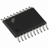
74ACT273MTC Fairchild Semiconductor, 74ACT273MTC Datasheet - Page 4

74ACT273MTC
Manufacturer Part Number
74ACT273MTC
Description
IC FLIP FLOP OCT D TYPE 20-TSSOP
Manufacturer
Fairchild Semiconductor
Series
74ACTr
Type
D-Type Busr
Datasheet
1.74ACT273MTC.pdf
(7 pages)
Specifications of 74ACT273MTC
Function
Master Reset
Output Type
Non-Inverted
Number Of Elements
1
Number Of Bits Per Element
8
Frequency - Clock
189MHz
Delay Time - Propagation
6.5ns
Trigger Type
Positive Edge
Current - Output High, Low
24mA, 24mA
Voltage - Supply
4.5 V ~ 5.5 V
Operating Temperature
-40°C ~ 85°C
Mounting Type
Surface Mount
Package / Case
20-TSSOP
Number Of Circuits
8
Logic Family
74ACT
Logic Type
D-Type Flip-Flop
Polarity
Non-Inverting
Input Type
Single-Ended
Propagation Delay Time
8.5 ns
High Level Output Current
- 24 mA
Low Level Output Current
24 mA
Supply Voltage (max)
5.5 V
Maximum Operating Temperature
+ 85 C
Mounting Style
SMD/SMT
Minimum Operating Temperature
- 40 C
Supply Voltage (min)
4.5 V
Lead Free Status / RoHS Status
Lead free / RoHS Compliant
FM3565 Rev. A.1
The output multiplexer logic determines what value is actually
output to the Y-port. The above table describes all the
combinations.
The IIC Interface is a standard slave interface. As such, the device
will not generate its own clock. Data can be read from and written
into the device. Commands for reading and writing the registers
are generated by the Master.
This protocol uniquely defines START and STOP conditions. A
START condition is defined as a HIGH to LOW transition of the
SDA signal while SCL is HIGH. A STOP condition is defined as a
LOW to HIGH transition of the SDA signal while SCL is HIGH.
These are shown in Figure 2.
The device uses 7-bit addressing. The address has been defined
as 1001 110 if the ASEL input is ‘1’ and 0110 111 if the ASEL input
is ‘0’. The address byte is the first byte of data sent after a start
condition. This is the only address that this device will respond to.
The device will not respond to the general call address 0000 000.
SDA
SCL
OVRD
0
0
1
1
1
Condition
START
MUXSEL
0
1
0
0
1
A/B
X
X
X
0
1
all 0's
Mux_inputs
From Non-volatile
register (SOPRB)
From Non-volatile
register (SOPRA)
Mux_inputs
Mux_outputs
Condition
STOP
Data can be read from both of the internal registers. All reads are
non-destructive and do not change the value in the register or the
internal state of the device. When a start condition is received with
a read request, both registers can be read out in the following
sequence:
(1) SOPRA: Serial Output Port Register A
(2) SPORB: Serial Output Port Register B
(3) PIPR: PORT-I Value
If so desired, only the SOPRA register can be read. This is
accomplished by issuing a stop command after the acknowledge
bit for the first byte is read. If no stop is issued, the device will output
the registers in the above sequence.
Data is written to the SOPR registers through the serial port
interface. When a write request is received with the Start Address,
it is assumed that the intent is to write to the SOPR registers. The
value placed in the least 6 significant bits of the register contain the
new code to be placed in the SOPR A/B registers. The value of the
two most significant bits must contain the address of the destina-
tion register SOPRA or SOPRB.
The internal non-volatile latch takes about 10 ms to update its
data.
xx = Register Selection bits (MXSB and MXSA) xx = 00 selects
SOPRA, 01 selects SOPRB
S Address R A Register A Register A Register A P
S Address W A Register A S
S
S
S Address R A Register A S Address W A Register A P
S 1001110 1 A 00bbbbbb A S 1001110 0 A xxbbbbbb A P
1001110
1001110
Slave
Slave
Slave
1 A 00bbbbbb A 00bbbbbb A 00bbbbbb A P
0 A xxbbbbbb A S
SOPRA
SOPRA
SOPRx
SOPRB
Slave
www.fairchildsemi.com
www.fairchildsemi.com
PIPR
SOPRx


