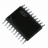
74HCT273PW,112 NXP Semiconductors, 74HCT273PW,112 Datasheet - Page 15

74HCT273PW,112
Manufacturer Part Number
74HCT273PW,112
Description
IC D-TYPE FF POS-EDG-TRG 20TSSOP
Manufacturer
NXP Semiconductors
Series
74HCTr
Type
D-Type Busr
Datasheet
1.74HC273PW118.pdf
(26 pages)
Specifications of 74HCT273PW,112
Function
Master Reset
Output Type
Non-Inverted
Number Of Elements
1
Number Of Bits Per Element
8
Frequency - Clock
36MHz
Delay Time - Propagation
15ns
Trigger Type
Positive Edge
Current - Output High, Low
4mA, 4mA
Voltage - Supply
4.5 V ~ 5.5 V
Operating Temperature
-40°C ~ 125°C
Mounting Type
Surface Mount
Package / Case
20-TSSOP
Logic Family
HCT
Technology
CMOS
Number Of Bits
8
Number Of Elements
1
Clock-edge Trigger Type
Positive-Edge
Polarity
Non-Inverting
Operating Supply Voltage (typ)
5V
Package Type
TSSOP
Propagation Delay Time
51ns
Low Level Output Current
4mA
High Level Output Current
-4mA
Frequency (max)
20MHz
Operating Supply Voltage (min)
4.5V
Operating Supply Voltage (max)
5.5V
Operating Temp Range
-40C to 125C
Operating Temperature Classification
Automotive
Mounting
Surface Mount
Pin Count
20
Lead Free Status / RoHS Status
Lead free / RoHS Compliant
Other names
74HCT273PW
74HCT273PW
935185820112
74HCT273PW
935185820112
Philips Semiconductors
Table 10:
Voltages are referenced to GND (ground = 0 V); t
Figure
[1]
74HC_HCT273_3
Product data sheet
Symbol Parameter
t
t
t
f
C
T
t
t
t
t
t
t
t
t
t
f
T
t
t
t
t
t
t
t
t
t
f
rec
su
h
max
PHL
PLH
PHL
THL
TLH
W
rec
su
h
max
PHL
PLH
PHL
THL
TLH
W
rec
su
h
max
amb
amb
PD
,
,
,
,
C
P
f
f
C
V
N = number of inputs switching;
i
o
D
CC
= 40 C to +85 C
= 40 C to +125 C
PD
= input frequency in MHz;
L
= output frequency in MHz;
10.
= output load capacitance in pF;
= C
is used to determine the dynamic power dissipation (P
= supply voltage in V;
recovery time MR to CP
set-up time Dn to CP
hold time Dn to CP
maximum input clock frequency
power dissipation capacitance
propagation delay CP to Qn
HIGH-to-LOW propagation delay
MR to Qn
output transition time
pulse width
recovery time MR to CP
set-up time Dn to CP
hold time Dn to CP
maximum input clock frequency
propagation delay CP to Qn
HIGH-to-LOW propagation delay
MR to Qn
output transition time
pulse width
recovery time MR to CP
set-up time Dn to CP
hold time Dn to CP
maximum input clock frequency
PD
Dynamic characteristics 74HCT273
clock HIGH or LOW
master reset LOW
clock HIGH or LOW
master reset LOW
V
CC
2
f
i
N + (C
L
V
CC
2
f
o
) where:
Conditions
V
V
V
see
per flip-flop; V
V
V
V
V
V
V
V
V
V
V
V
V
V
V
V
V
V
V
CC
CC
CC
CC
CC
CC
CC
CC
CC
CC
CC
CC
CC
CC
CC
CC
CC
CC
CC
CC
CC
V
V
r
CC
CC
Rev. 03 — 24 January 2006
Figure 7
…continued
= t
= 4.5 V; see
= 4.5 V; see
= 4.5 V; see
= 4.5 V; see
= 4.5 V; see
= 4.5 V; see
= 4.5 V; see
= 4.5 V; see
= 4.5 V; see
= 4.5 V; see
= 4.5 V; see
= 4.5 V; see
= 4.5 V; see
= 4.5 V; see
= 4.5 V; see
= 4.5 V; see
= 4.5 V; see
= 4.5 V; see
= 4.5 V; see
= 4.5 V; see
= 4.5 V; see
= 4.5 V
= 5.0 V; C
f
= 6 ns; C
D
in W).
I
Octal D-type flip-flop with reset; positive-edge trigger
= GND to (V
L
Figure 8
Figure 9
Figure 9
Figure 7
Figure 8
Figure 7
Figure 7
Figure 8
Figure 8
Figure 9
Figure 9
Figure 7
Figure 7
Figure 8
Figure 7
Figure 7
Figure 8
Figure 8
Figure 9
Figure 9
Figure 7
L
= 15 pF
= 50 pF unless otherwise specified; for test circuit see
CC
74HC273; 74HCT273
1.5 V)
[1]
Min
+10
12
+3
30
-
-
-
-
-
20
20
13
15
3
24
-
-
-
24
24
15
18
3
20
© Koninklijke Philips Electronics N.V. 2006. All rights reserved.
Typ
5
56
36
23
-
-
-
-
-
-
-
-
-
-
-
-
-
-
-
-
-
-
2
4
Max
-
-
-
-
-
-
38
43
19
-
-
-
-
-
-
45
51
22
-
-
-
-
-
-
Unit
ns
ns
ns
MHz
MHz
pF
ns
ns
ns
ns
ns
ns
ns
ns
MHz
ns
ns
ns
ns
ns
ns
ns
ns
MHz
15 of 26


