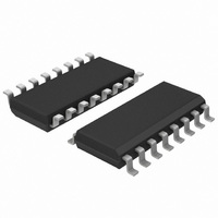
74HC173D,653 NXP Semiconductors, 74HC173D,653 Datasheet - Page 2

74HC173D,653
Manufacturer Part Number
74HC173D,653
Description
IC QUAD D F-F POS-EDGE 16SOIC
Manufacturer
NXP Semiconductors
Series
74HCr
Type
D-Type Busr
Datasheet
1.74HCT173DB112.pdf
(10 pages)
Specifications of 74HC173D,653
Output Type
Tri-State Non Inverted
Package / Case
16-SOIC (3.9mm Width)
Function
Master Reset
Number Of Elements
1
Number Of Bits Per Element
4
Frequency - Clock
95MHz
Delay Time - Propagation
16ns
Trigger Type
Positive Edge
Voltage - Supply
2 V ~ 6 V
Operating Temperature
-40°C ~ 125°C
Mounting Type
Surface Mount
Number Of Circuits
1
Logic Family
HC
Logic Type
D-Type Edge Triggered Flip-Flop
Polarity
Non-Inverting
Input Type
Single-Ended
Propagation Delay Time
17 ns at 5 V
High Level Output Current
- 7.8 mA
Low Level Output Current
7.8 mA
Supply Voltage (max)
6 V
Maximum Operating Temperature
+ 125 C
Mounting Style
SMD/SMT
Minimum Operating Temperature
- 40 C
Supply Voltage (min)
2 V
Technology
CMOS
Number Of Bits
4
Number Of Elements
1
Clock-edge Trigger Type
Positive-Edge
Operating Supply Voltage (typ)
5V
Package Type
SO
Operating Supply Voltage (min)
2V
Operating Supply Voltage (max)
6V
Operating Temp Range
-40C to 125C
Operating Temperature Classification
Automotive
Mounting
Surface Mount
Pin Count
16
Lead Free Status / RoHS Status
Lead free / RoHS Compliant
Current - Output High, Low
-
Lead Free Status / Rohs Status
Lead free / RoHS Compliant
Other names
568-4558-2
74HC173D-T
74HC173D-T
933714560653
74HC173D-T
74HC173D-T
933714560653
Philips Semiconductors
FEATURES
GENERAL DESCRIPTION
The 74HC/HCT173 are high-speed Si-gate CMOS devices
and are pin compatible with low power Schottky TTL
(LSTTL). They are specified in compliance with JEDEC
standard no. 7A.
The 74HC/HCT173 are 4-bit parallel load registers with
clock enable control, 3-state buffered outputs (Q
and master reset (MR).
When the two data enable inputs (E
data on the D
QUICK REFERENCE DATA
GND = 0 V; T
Notes
1. C
2. For HC the condition is V
ORDERING INFORMATION
See
December 1990
t
f
C
C
PHL
max
Gated input enable for hold (do nothing) mode
Gated output enable control
Edge-triggered D-type register
Asynchronous master reset
Output capability: bus driver
I
Quad D-type flip-flop; positive-edge trigger; 3-state
I
PD
CC
f
f
C
V
For HCT the condition is V
SYMBOL
i
o
“74HC/HCT/HCU/HCMOS Logic Package Information”
/ t
CC
PD
L
category: MSI
= output frequency in MHz
= input frequency in MHz
(C
PLH
= output load capacitance in pF
P
is used to determine the dynamic power dissipation (P
= supply voltage in V
L
D
= C
V
amb
CC
n
PD
inputs is loaded into the register
2
= 25 C; t
propagation delay
maximum clock frequency
input capacitance
power dissipation
capacitance per flip-flop
V
f
CP to Q
MR to Q
o
CC
) = sum of outputs
2
f
r
PARAMETER
i
n
= t
n
I
I
f
= GND to V
= GND to V
= 6 ns
(C
1
L
and E
V
CC
2
2
CC
) are LOW, the
CC
f
o
1.5 V
) where:
0
to Q
C
notes 1 and 2
L
3
= 15 pF; V
)
2
CONDITIONS
.
synchronously with the LOW-to-HIGH clock (CP)
transition. When one or both E
set-up time prior to the LOW-to-HIGH clock transition, the
register will retain the previous data. Data inputs and clock
enable inputs are fully edge-triggered and must be stable
only one set-up time prior to the LOW-to-HIGH clock
transition.
The master reset input (MR) is an active HIGH
asynchronous input. When MR is HIGH, all four flip-flops
are reset (cleared) independently of any other input
condition.
The 3-state output buffers are controlled by a 2-input NOR
gate. When both output enable inputs (OE
LOW, the data in the register is presented to the Q
outputs. When one or both OE
outputs are forced to a high impedance OFF-state. The
3-state output buffers are completely independent of the
register operation; the OE
clock and reset operations.
D
in W):
CC
= 5 V
17
13
88
3.5
20
HC
n
transition does not affect the
TYPICAL
n
n
inputs are HIGH one
inputs are HIGH, the
74HC/HCT173
17
17
88
3.5
20
Product specification
HCT
1
and OE
ns
ns
MHz
pF
pF
UNIT
n
2
) are


