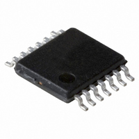
74LVC04APW,118 NXP Semiconductors, 74LVC04APW,118 Datasheet - Page 3

74LVC04APW,118
Manufacturer Part Number
74LVC04APW,118
Description
IC INVERTER HEX 5V TTL 14TSSOP
Manufacturer
NXP Semiconductors
Series
74LVCr
Datasheet
1.74LVC04AD118.pdf
(15 pages)
Specifications of 74LVC04APW,118
Number Of Circuits
6
Logic Type
Inverter
Package / Case
14-TSSOP
Number Of Inputs
1
Current - Output High, Low
12mA, 12mA
Voltage - Supply
2.7 V ~ 3.6 V
Operating Temperature
-40°C ~ 125°C
Mounting Type
Surface Mount
Logic Family
74LVC
High Level Output Current
- 24 mA
Low Level Output Current
24 mA
Propagation Delay Time
14 ns
Supply Voltage (max)
3.6 V
Supply Voltage (min)
1.2 V
Maximum Operating Temperature
+ 125 C
Minimum Operating Temperature
- 40 C
Mounting Style
SMD/SMT
Operating Supply Voltage
1.2 V to 3.6 V
Logical Function
Inverter
Number Of Elements
6
Operating Supply Voltage (typ)
1.8/2.5/3.3V
Package Type
TSSOP
Operating Temp Range
-40C to 125C
Pin Count
14
Quiescent Current
40uA
Technology
CMOS
Mounting
Surface Mount
Operating Temperature Classification
Automotive
Operating Supply Voltage (max)
3.6V
Operating Supply Voltage (min)
1.2V
Lead Free Status / RoHS Status
Lead free / RoHS Compliant
Lead Free Status / RoHS Status
Lead free / RoHS Compliant, Lead free / RoHS Compliant
Other names
568-1574-2
74LVC04APW-T
935242420118
74LVC04APW-T
935242420118
NXP Semiconductors
Table 2.
6. Functional description
Table 3.
[1]
7. Limiting values
Table 4.
In accordance with the Absolute Maximum Rating System (IEC 60134). Voltages are referenced to GND (ground = 0 V).
[1]
74LVC04A
Product data sheet
Symbol
1A
1Y
2A
2Y
3A
3Y
GND
4Y
4A
5Y
5A
6Y
6A
V
Input nA
L
H
Symbol
V
I
V
I
V
I
I
I
T
P
IK
OK
O
CC
GND
stg
CC
CC
I
O
tot
H = HIGH voltage level; L = LOW voltage level
The minimum input voltage ratings may be exceeded if the input current ratings are observed.
Pin description
Function table
Limiting values
Parameter
supply voltage
input clamping current
input voltage
output clamping current
output voltage
output current
supply current
ground current
storage temperature
total power dissipation
5.2 Pin description
Pin
1
2
3
4
5
6
7
8
9
10
11
12
13
14
[1]
All information provided in this document is subject to legal disclaimers.
Conditions
V
V
V
T
Description
data input
data output
data input
data output
data input
data output
ground (0 V)
data output
data input
data output
data input
data output
data input
supply voltage
amb
I
O
O
< 0
Rev. 7 — 1 February 2011
> V
= 0 V to V
= −40 °C to +125 °C
CC
or V
CC
O
Output nY
H
L
< 0
[1]
[2]
[3]
Min
−0.5
−50
−0.5
-
−0.5
-
-
−100
−65
-
Max
+6.5
-
+6.5
±50
V
±50
100
-
+150
500
74LVC04A
CC
© NXP B.V. 2011. All rights reserved.
+ 0.5
Hex inverter
Unit
V
mA
V
mA
V
mA
mA
mA
°C
mW
3 of 15


