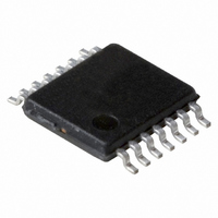
74LVC06APW,118 NXP Semiconductors, 74LVC06APW,118 Datasheet - Page 6

74LVC06APW,118
Manufacturer Part Number
74LVC06APW,118
Description
IC INVERTER HEX 1INPUT 14TSSOP
Manufacturer
NXP Semiconductors
Series
74LVCr
Datasheet
1.74LVC06AD118.pdf
(14 pages)
Specifications of 74LVC06APW,118
Package / Case
14-TSSOP
Logic Type
Inverter with Open Drain
Number Of Inputs
1
Number Of Circuits
6
Current - Output High, Low
32mA, 32mA
Voltage - Supply
1.65 V ~ 5.5 V
Operating Temperature
-40°C ~ 125°C
Mounting Type
Surface Mount
Logic Family
LVC
Number Of Channels Per Chip
6
Polarity
Inverting
Supply Voltage (max)
5.5 V
Supply Voltage (min)
1.65 V
Maximum Operating Temperature
+ 125 C
Mounting Style
SMD/SMT
Input Bias Current (max)
10 uA
Low Level Output Current
32 mA
Minimum Operating Temperature
- 40 C
Output Type
Open Drain
Propagation Delay Time
2.3 ns (Typ) @ 3.3 V
Number Of Lines (input / Output)
6 / 6
Logical Function
Buffer/Driver
Number Of Elements
6
Number Of Channels
6
Number Of Outputs
6
Operating Supply Voltage (typ)
1.8/2.5/3.3/5V
Package Type
TSSOP
Operating Supply Voltage (max)
5.5V
Operating Supply Voltage (min)
1.65V
Quiescent Current
10uA
Technology
CMOS
Pin Count
14
Mounting
Surface Mount
Operating Temp Range
-40C to 125C
Operating Temperature Classification
Automotive
Lead Free Status / RoHS Status
Lead free / RoHS Compliant
Lead Free Status / RoHS Status
Lead free / RoHS Compliant, Lead free / RoHS Compliant
Other names
568-4490-2
74LVC06APW-T
74LVC06APW-T
935265480118
74LVC06APW-T
74LVC06APW-T
935265480118
Available stocks
Company
Part Number
Manufacturer
Quantity
Price
Philips Semiconductors
DC CHARACTERISTICS
At recommended operating conditions; voltages are referenced to GND (ground = 0 V).
2003 Nov 27
T
V
V
V
I
I
I
I
T
V
V
SYMBOL
LI
OZ
off
CC
amb
I
amb
IH
IL
OL
IH
IL
Hex inverter with open-drain outputs
CC
= 40 to +85 C
= 40 to +125 C
HIGH-level input
voltage
LOW-level input voltage
LOW-level output
voltage
input leakage current
output leakage current
power-off leakage
current
quiescent supply
current
additional quiescent
supply current per input
pin
HIGH-level input
voltage
LOW-level input voltage
PARAMETER
V
V
V
V
V
V
I
V
I
O
O
I
I
I
O
I
I
I
I
I
I
I
I
I
= V
= 5.5 V or GND
= V
or V
= V
= 0
= V
= 0
O
O
O
O
O
O
= 5.5 V or GND
= 100 A
= 4 mA
= 8 mA
= 12 mA
= 24 mA
= 32 mA
IH
IH
CC
CC
OTHER
O
TEST CONDITIONS
;
or V
= 5.5 V
or GND;
0.6 V;
IL
6
1.65 to 1.95
2.3 to 2.7
2.7 to 3.6
4.5 to 5.5
1.65 to 1.95
2.3 to 2.7
2.7 to 3.6
4.5 to 5.5
1.65 to 5.5
1.65
2.3
2.7
3.0
4.5
1.65 to 5.5
1.65 to 5.5
0
5.5
2.3 to 5.5
1.65 to 1.95
2.3 to 2.7
2.7 to 3.6
4.5 to 5.5
1.65 to 1.95
2.3 to 2.7
2.7 to 3.6
4.5 to 5.5
V
CC
(V)
V
1.7
2.0
0.7
0.65 x V
1.7
2.0
0.7
CC
MIN.
V
V
CC
CC
CC
0.1
0.1
5
TYP.
0.1
0.1
(1)
GND
0.7
0.8
0.30
0.20
0.45
0.3
0.4
0.55
0.55
10
500
0.35
0.7
0.8
0.30
Product specification
5
10
10
74LVC06A
MAX.
V
V
V
CC
CC
CC
V
V
V
V
V
V
V
V
V
V
V
V
V
V
V
V
V
V
V
V
V
V
UNIT
A
A
A
A
A


