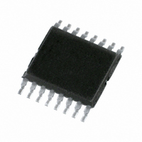
74HC366PW,112 NXP Semiconductors, 74HC366PW,112 Datasheet - Page 8

74HC366PW,112
Manufacturer Part Number
74HC366PW,112
Description
IC INVERTER HEX 1-INPUT 16TSSOP
Manufacturer
NXP Semiconductors
Series
74HCr
Datasheet
1.74HC366PW112.pdf
(19 pages)
Specifications of 74HC366PW,112
Logic Type
Inverter
Number Of Inputs
1
Number Of Circuits
6
Current - Output High, Low
7.8mA, 7.8mA
Voltage - Supply
2 V ~ 6 V
Operating Temperature
-40°C ~ 125°C
Mounting Type
Surface Mount
Package / Case
16-TSSOP
Logic Family
HC
Number Of Channels Per Chip
6
Polarity
Inverting
Supply Voltage (max)
6 V
Supply Voltage (min)
2 V
Maximum Operating Temperature
+ 125 C
Mounting Style
SMD/SMT
High Level Output Current
- 7.8 mA
Low Level Output Current
7.8 mA
Minimum Operating Temperature
- 40 C
Number Of Lines (input / Output)
6 / 6
Output Type
3-State
Propagation Delay Time
100 ns at 2 V, 20 ns at 4.5 V, 17 ns at 6 V
Lead Free Status / RoHS Status
Lead free / RoHS Compliant
Other names
74HC366PW
74HC366PW
935283208112
74HC366PW
935283208112
NXP Semiconductors
Table 7.
At recommended operating conditions; voltages are referenced to GND (ground = 0 V).
10. Dynamic characteristics
Table 8.
Voltages are referenced to GND (ground = 0 V); C
74HC_HCT366_3
Product data sheet
Symbol Parameter
I
I
T
V
V
V
V
I
I
I
Symbol Parameter
T
t
t
OZ
CC
I
OZ
CC
pd
en
I
amb
I
amb
IH
IL
OH
OL
CC
CC
= 40 C to +125 C
= 25 C
OFF-state output current V
supply current
additional supply current V
HIGH-level input voltage V
LOW-level input voltage
HIGH-level output
voltage
LOW-level output voltage V
input leakage current
OFF-state output current V
supply current
additional supply current V
propagation delay
enable time
Static characteristics 74HCT366
Dynamic characteristics 74HC366
Conditions
inputs at GND or V
V
V
V
V
inputs at GND or V
V
Conditions
nA to nY; see
OEn to nY; see
I
I
I
CC
CC
I
I
I
I
I
I
pins nA
pin OE1
pin OE2
I
I
I
I
pins nA
pin OE1
pin OE2
V
V
V
V
V
V
V
= V
= V
= V
= V
= V
= V
= V
= V
= V
O
O
O
O
CC
CC
CC
CC
CC
CC
CC
= 4.5 V to 5.5 V
= 4.5 V to 5.5 V
= 20 A
= 6.0 mA
= 20 A
= 6.0 mA
IH
CC
CC
IH
IH
CC
IH
CC
CC
= 2.0 V
= 4.5 V
= 5 V; C
= 6.0 V
= 2.0 V
= 4.5 V
= 6.0 V
or V
or V
or V
or V
or GND; I
or GND; V
or GND; I
…continued
2.1 V; other inputs at V
2.1 V; other inputs at V
Rev. 03 — 21 November 2006
IL
IL
IL
IL
L
; V
; V
; V
; V
Figure 6
= 50 pF unless otherwise specified; see test circuit
L
Figure 7
= 15 pF
O
CC
CC
O
= V
= V
O
O
CC
CC
CC
= 4.5 V
= 4.5 V
= 0 A; V
= 0 A; V
; I
; I
CC
CC
= 5.5 V
O
O
or GND per input pin; other
= 0 A; V
or GND per input pin; other
= 0 A; V
CC
CC
= 5.5 V
= 5.5 V
CC
CC
CC
CC
= 5.5 V
= 5.5 V
or GND; I
or GND; I
74HC366; 74HCT366
Hex buffer/line driver; 3-state; inverting
O
O
= 0 A
= 0 A
[1]
[2]
Min
-
-
-
-
2.0
-
4.4
3.7
-
-
-
-
-
-
-
-
Min
-
-
-
-
-
-
-
Figure
Typ
-
-
-
-
-
-
-
-
-
-
-
-
-
-
-
-
Typ
33
12
10
10
44
16
13
© NXP B.V. 2006. All rights reserved.
Max
80
450
450
400
-
0.8
-
-
0.1
0.4
160
490
490
441
8.
Max
100
20
-
17
150
30
26
5.0
1.0
10.0
Unit
ns
ns
ns
ns
ns
ns
ns
Unit
V
V
V
V
V
V
8 of 19
A
A
A
A
A
A
A
A
A
A
A


