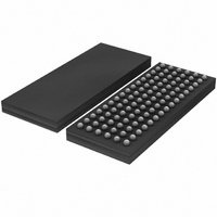
74LVCH32373AEC,551 NXP Semiconductors, 74LVCH32373AEC,551 Datasheet - Page 7

74LVCH32373AEC,551
Manufacturer Part Number
74LVCH32373AEC,551
Description
IC 32BIT TRANSP D LATCH 96LFBGA
Manufacturer
NXP Semiconductors
Series
74LVCHr
Datasheet
1.74LVCH32373AECG5.pdf
(14 pages)
Specifications of 74LVCH32373AEC,551
Logic Type
D-Type Transparent Latch
Circuit
8:8
Output Type
Tri-State
Voltage - Supply
2.7 V ~ 3.6 V
Independent Circuits
4
Delay Time - Propagation
3ns
Current - Output High, Low
24mA, 24mA
Operating Temperature
-40°C ~ 85°C
Mounting Type
Surface Mount
Package / Case
96-LFBGA
Lead Free Status / RoHS Status
Lead free / RoHS Compliant
Other names
74LVCH32373AEC-S
74LVCH32373AEC-S
935264448551
74LVCH32373AEC-S
935264448551
Available stocks
Company
Part Number
Manufacturer
Quantity
Price
Company:
Part Number:
74LVCH32373AEC,551
Manufacturer:
NXP Semiconductors
Quantity:
10 000
Philips Semiconductors
DC CHARACTERISTICS
At recommended operating conditions; voltages are referenced to GND (ground = 0 V).
Notes
1. All typical values are measured at V
2. For bushold parts, the bushold circuit is switched off when V
3. For data inputs only, control inputs do not have a bushold circuit.
4. The specified sustaining current at the data inputs holds the input below the specified V
5. The specified overdrive current at the data input forces the data input to the opposite logic input state.
2004 May 19
T
V
V
V
V
I
I
I
I
I
I
I
I
SYMBOL
LI
OZ
off
CC
BH
BHH
BHLO
BHHO
amb
I
IH
IL
OH
OL
32-bit transparent D-type latch with
5 V tolerant inputs/outputs; 3-state
CC
= 40 C to +85 C; note 1
HIGH-level input voltage
LOW-level input voltage
HIGH-level output voltage
LOW-level output voltage
input leakage current
3-state output OFF-state
current
power-off leakage supply
current
quiescent supply current
additional quiescent supply
current per input pin
bushold LOW sustaining
current
bushold HIGH sustaining
current
bushold LOW overdrive
current
bushold HIGH overdrive
current
PARAMETER
CC
V
V
V
note 2
V
V
note 2
V
V
I
V
I
V
notes 3 and 4
V
notes 3 and 4
notes 3 and 5
notes 3 and 5
O
O
= 3.3 V and T
I
I
I
I
O
I
I
I
I
I
I
I
I
I
I
I
I
= V
= V
= 5.5 V or GND;
= V
or V
= V
= 0 A
= V
= 0 A
= 0.8 V;
= 2.0 V;
O
O
O
O
O
O
O
= 5.5 V or GND;
= 100 A
= 12 mA
= 18 mA
= 24 mA
= 100 A
= 12 mA
= 24 mA
IH
IH
IH
CC
CC
OTHER
TEST CONDITIONS
O
or V
or V
or V
= 5.5 V
or GND;
0.6 V;
IL
IL
IL
;
amb
7
= 25 C.
1.2
2.7 to 3.6
1.2
2.7 to 3.6
2.7 to 3.6
2.7
3.0
3.0
2.7 to 3.6
2.7
3.0
3.6
3.6
0.0
3.6
2.7 to 3.6
3.0
3.0
3.6
3.6
I
> V
V
CC
CC
(V)
allowing 5.5 V on the input pin.
V
2.0
V
V
V
V
75
500
75
500
CC
CC
CC
CC
CC
MIN.
0.2
0.5
0.6
0.8
V
GND
0.1
0.1
0.1
5
I
74LVCH32373A
0.1
CC
level.
TYP.
Product specification
GND
0.8
0.20
0.40
0.55
40
500
MAX.
5
5
10
V
V
V
V
V
V
V
V
V
V
V
UNIT
A
A
A
A
A
A
A
A
A


