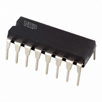
74HC595N,112 NXP Semiconductors, 74HC595N,112 Datasheet - Page 2

74HC595N,112
Manufacturer Part Number
74HC595N,112
Description
IC SHIFT REGISTER 8BIT 16DIP
Manufacturer
NXP Semiconductors
Series
74HCr
Datasheet
1.74HC595D118.pdf
(28 pages)
Specifications of 74HC595N,112
Package / Case
16-DIP (0.300", 7.62mm)
Logic Type
Shift Register
Output Type
Standard
Function
Serial to Parallel
Number Of Elements
1
Number Of Bits Per Element
8
Voltage - Supply
2 V ~ 6 V
Operating Temperature
-40°C ~ 125°C
Mounting Type
Through Hole
Counting Sequence
Serial to Serial/Parallel
Number Of Circuits
1
Logic Family
74HC
Propagation Delay Time
175 ns, 35 ns, 30 ns
Supply Voltage (max)
6 V
Maximum Operating Temperature
+ 125 C
Minimum Operating Temperature
- 40 C
Mounting Style
SMD/SMT
Operating Supply Voltage
2 V to 6 V
Lead Free Status / RoHS Status
Lead free / RoHS Compliant
Lead Free Status / RoHS Status
Lead free / RoHS Compliant, Lead free / RoHS Compliant
Other names
568-1484-5
74HC595N
935009150112
74HC595N
935009150112
Philips Semiconductors
FEATURES
APPLICATIONS
QUICK REFERENCE DATA
GND = 0 V; T
Notes
1. C
2. For 74HC595 the condition is V
2003 Jun 25
t
f
C
C
SYMBOL
PHL
max
8-bit serial input
8-bit serial or parallel output
Storage register with 3-state outputs
Shift register with direct clear
100 MHz (typical) shift out frequency
ESD protection:
HBM EIA/JESD22-A114-A exceeds 2000 V
MM EIA/JESD22-A115-A exceeds 200 V.
Serial-to-parallel data conversion
Remote control holding register.
I
PD
8-bit serial-in, serial or parallel-out shift
register with output latches; 3-state
P
f
f
C
V
N = total load switching outputs;
For 74HCT595 the condition is V
i
o
/t
(C
D
CC
PD
= input frequency in MHz;
L
PLH
= output frequency in MHz;
= output load capacitance in pF;
= C
L
is used to determine the dynamic power dissipation (P
= supply voltage in Volts;
PD
V
CC
propagation delay
maximum clock frequency SH_CP and ST_CP
input capacitance
power dissipation capacitance per package
amb
SH_CP to Q7’
SH_CP to Qn
MR to Q7’
2
V
CC
= 25 C; t
f
o
2
) = sum of the outputs.
f
i
N + (C
r
= t
PARAMETER
f
= 6 ns.
L
I
= GND to V
I
= GND to V
V
CC
2
f
o
) where:
CC
CC
.
1.5 V.
2
DESCRIPTION
The 74HC/HCT595 are high-speed Si-gate CMOS devices
and are pin compatible with low power Schottky TTL
(LSTTL). They are specified in compliance with JEDEC
standard no. 7A.
The 74HC/HCT595 is an 8-stage serial shift register with a
storage register and 3-state outputs. The shift register and
storage register have separate clocks.
Data is shifted on the positive-going transitions of the
SH_CP input. The data in each register is transferred to
the storage register on a positive-going transition of the
ST_CP input. If both clocks are connected together, the
shift register will always be one clock pulse ahead of the
storage register.
The shift register has a serial input (DS) and a serial
standard output (Q7’) for cascading. It is also provided
with asynchronous reset (active LOW) for all 8 shift
register stages. The storage register has 8 parallel 3-state
bus driver outputs. Data in the storage register appears at
the output whenever the output enable input (OE) is LOW.
C
notes 1 and 2
D
L
in W).
= 50 pF; V
CONDITIONS
CC
= 4.5 V
74HC595; 74HCT595
19
20
100
100
3.5
115
74HC
TYPICAL
Product specification
25
24
52
57
3.5
130
74HCT
ns
ns
ns
MHz
pF
pF
UNIT


