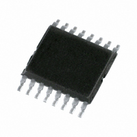
74HC595PW,118 NXP Semiconductors, 74HC595PW,118 Datasheet - Page 4

74HC595PW,118
Manufacturer Part Number
74HC595PW,118
Description
IC SHIFT REGISTER 8BIT 16TSSOP
Manufacturer
NXP Semiconductors
Series
74HCr
Type
Not Requiredr
Datasheet
1.74HC595D118.pdf
(28 pages)
Specifications of 74HC595PW,118
Package / Case
16-TSSOP
Logic Type
Shift Register
Output Type
Standard
Function
Serial to Parallel
Number Of Elements
1
Number Of Bits Per Element
8
Voltage - Supply
2 V ~ 6 V
Operating Temperature
-40°C ~ 125°C
Mounting Type
Surface Mount
Counting Sequence
Serial to Serial/Parallel
Number Of Circuits
1
Logic Family
74HC
Propagation Delay Time
175 ns, 35 ns, 30 ns
Supply Voltage (max)
6 V
Maximum Operating Temperature
+ 125 C
Minimum Operating Temperature
- 40 C
Mounting Style
SMD/SMT
Operating Supply Voltage
2 V to 6 V
Technology
CMOS
Number Of Elements
1
Number Of Bits
8
Logical Function
Shift Register
Operating Supply Voltage (typ)
5V
Package Type
TSSOP
Operating Temp Range
-40C to 125C
Operating Supply Voltage (min)
2V
Operating Supply Voltage (max)
6V
Operating Temperature Classification
Automotive
Mounting
Surface Mount
Pin Count
16
Lead Free Status / RoHS Status
Lead free / RoHS Compliant
Lead Free Status / RoHS Status
Lead free / RoHS Compliant, Lead free / RoHS Compliant
Other names
568-2263-2
74HC595PW-T
935188520118
74HC595PW-T
935188520118
Available stocks
Company
Part Number
Manufacturer
Quantity
Price
Company:
Part Number:
74HC595PW,118
Manufacturer:
NXP Semiconductors
Quantity:
1 250
Philips Semiconductors
PINNING
2003 Jun 25
handbook, halfpage
8-bit serial-in, serial or parallel-out shift
register with output latches; 3-state
Fig.1
PIN
10
11
12
13
14
15
16
1
2
3
4
5
6
7
8
9
Pin configuration DIP16, SO16 and
(T)SSOP16.
GND
Q1
Q2
Q3
Q4
Q5
Q6
Q7
Q1
Q2
Q3
Q4
Q5
Q6
Q7
GND
Q7’
MR
SH_CP
ST_CP
OE
DS
Q0
V
CC
SYMBOL
1
2
3
4
5
6
7
8
595
MLA001
parallel data output
parallel data output
parallel data output
parallel data output
parallel data output
parallel data output
parallel data output
ground (0 V)
serial data output
master reset (active LOW)
shift register clock input
storage register clock input
output enable (active LOW)
serial data input
parallel data output
positive supply voltage
15
14
13
12
10
16
11
9
V CC
Q0
DS
OE
ST_CP
SH_CP
Q7'
MR
4
handbook, halfpage
(1) The die substrate is attached to this pad using conductive die
attach material. It can not be used as a supply pin or input.
DESCRIPTION
Fig.2 Pin configuration DHVQFN16.
Q2
Q3
Q4
Q5
Q6
Q7
Top view
2
3
4
5
6
7
74HC595; 74HCT595
GND
Q1
8
1
GND
V CC
(1)
Q7'
16
9
Product specification
MBL893
15
14
13
12
11
10
Q0
DS
OE
ST_CP
SH_CP
MR


