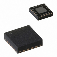
74LVC595ABQ,115 NXP Semiconductors, 74LVC595ABQ,115 Datasheet - Page 5

74LVC595ABQ,115
Manufacturer Part Number
74LVC595ABQ,115
Description
IC 8BIT SHIFT REGISTER 16HVQFN
Manufacturer
NXP Semiconductors
Series
74LVCr
Type
Not Requiredr
Datasheet
1.74LVC595ABQ115.pdf
(19 pages)
Specifications of 74LVC595ABQ,115
Package / Case
16-VQFN Exposed Pad, 16-HVQFN, 16-SQFN, 16-DHVQFN
Logic Type
Shift Register
Output Type
Standard
Function
Serial to Parallel
Number Of Elements
1
Number Of Bits Per Element
8
Voltage - Supply
1.65 V ~ 3.6 V
Operating Temperature
-40°C ~ 125°C
Mounting Type
Surface Mount
Counting Sequence
Serial to Serial/Parallel
Number Of Circuits
1
Logic Family
LVC
Propagation Delay Time
4.7 ns, 4 ns
Supply Voltage (max)
3.6 V
Maximum Operating Temperature
+ 125 C
Minimum Operating Temperature
- 40 C
Mounting Style
SMD/SMT
Operating Supply Voltage
1.8 V, 2.5 V, 3.3 V
Technology
CMOS
Number Of Elements
1
Number Of Bits
8
Logical Function
Shift Register
Operating Supply Voltage (typ)
1.8/2.5/3.3V
Operating Temp Range
-40C to 125C
Operating Supply Voltage (max)
3.6V
Operating Temperature Classification
Automotive
Mounting
Surface Mount
Pin Count
16
Lead Free Status / RoHS Status
Lead free / RoHS Compliant
Lead Free Status / RoHS Status
Lead free / RoHS Compliant, Lead free / RoHS Compliant
Other names
74LVC595ABQ-G
74LVC595ABQ-G
935282468115
74LVC595ABQ-G
935282468115
NXP Semiconductors
7. Functional description
Table 3.
[1]
8. Limiting values
Table 4.
In accordance with the Absolute Maximum Rating System (IEC 60134). Voltages are referenced to GND (ground = 0 V).
[1]
[2]
74LVC595A_1
Product data sheet
Input
SHCP STCP OE
X
X
X
X
Symbol
V
I
V
I
V
I
I
I
T
P
IK
OK
O
CC
GND
stg
CC
I
O
tot
H = HIGH voltage state;
L = LOW voltage state;
X = don’t care;
NC = no change;
Z = high-impedance OFF-state.
The input and output voltage ratings may be exceeded if the input and output current ratings are observed.
For SO16 packages: above 70 C the value of P
For TSSOP16 packages: above 60 C the value of P
For DHVQFN16 packages: above 60 C the value of P
= LOW-to-HIGH transition;
X
X
X
Function table
Limiting values
Parameter
supply voltage
input clamping current
input voltage
output clamping current
output voltage
output current
supply current
ground current
storage temperature
total power dissipation
L
L
H
L
L
L
MR
L
L
L
H
H
H
[1]
DS
X
X
X
H
X
X
Output
Q7S
L
L
L
Q6S
NC
Q6S
tot
Conditions
V
V
3-state
output HIGH or LOW state
V
T
Qn
NC
L
Z
NC
QnS
QnS
derates linearly with 8 mW/K.
amb
I
O
O
< 0 V
tot
Rev. 01 — 29 May 2007
> V
= 0 V to V
tot
derates linearly with 5.5 mW/K.
8-bit serial-in/serial-out or parallel-out shift register; 3-state
= 40 C to +125 C
derates linearly with 4.5 mW/K.
CC
Function
a LOW-state on MR only affects the shift register
empty shift register loaded into storage register
shift register clear; parallel outputs in high impedance OFF-state
logic HIGH-state shifted into shift register stage 0. Contents of all
shift register stages shifted through, e.g. previous state of stage 6
(internal Q6S) appears on the serial output (Q7S).
contents of shift register stages (internal QnS) are transferred to
the storage register and parallel output stages
contents of shift register shifted through; previous contents of the
shift register is transferred to the storage register and the parallel
output stages
or V
CC
O
< 0 V
[1]
[1]
[1]
[2]
Min
-
-
-
-
0.5
50
0.5
0.5
0.5
100
65
74LVC595A
Max
+6.5
-
+6.5
6.5
V
100
-
+150
500
50
50
CC
© NXP B.V. 2007. All rights reserved.
+ 0.5
Unit
V
mA
V
mA
V
V
mA
mA
mA
mW
C
5 of 19


