74LVC595ABQ,115 NXP Semiconductors, 74LVC595ABQ,115 Datasheet - Page 9
74LVC595ABQ,115
Manufacturer Part Number
74LVC595ABQ,115
Description
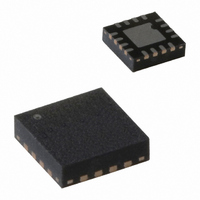
IC 8BIT SHIFT REGISTER 16HVQFN
Manufacturer
NXP Semiconductors
Series
74LVCr
Type
Not Requiredr
Datasheet
1.74LVC595ABQ115.pdf
(19 pages)
Specifications of 74LVC595ABQ,115
Package / Case
16-VQFN Exposed Pad, 16-HVQFN, 16-SQFN, 16-DHVQFN
Logic Type
Shift Register
Output Type
Standard
Function
Serial to Parallel
Number Of Elements
1
Number Of Bits Per Element
8
Voltage - Supply
1.65 V ~ 3.6 V
Operating Temperature
-40°C ~ 125°C
Mounting Type
Surface Mount
Counting Sequence
Serial to Serial/Parallel
Number Of Circuits
1
Logic Family
LVC
Propagation Delay Time
4.7 ns, 4 ns
Supply Voltage (max)
3.6 V
Maximum Operating Temperature
+ 125 C
Minimum Operating Temperature
- 40 C
Mounting Style
SMD/SMT
Operating Supply Voltage
1.8 V, 2.5 V, 3.3 V
Technology
CMOS
Number Of Elements
1
Number Of Bits
8
Logical Function
Shift Register
Operating Supply Voltage (typ)
1.8/2.5/3.3V
Operating Temp Range
-40C to 125C
Operating Supply Voltage (max)
3.6V
Operating Temperature Classification
Automotive
Mounting
Surface Mount
Pin Count
16
Lead Free Status / RoHS Status
Lead free / RoHS Compliant
Lead Free Status / RoHS Status
Lead free / RoHS Compliant, Lead free / RoHS Compliant
Other names
74LVC595ABQ-G
74LVC595ABQ-G
935282468115
74LVC595ABQ-G
935282468115


NXP Semiconductors
Table 7.
Voltages are referenced to GND (ground = 0 V). For test circuit see
[1]
[2]
[3]
[4]
[5]
[6]
74LVC595A_1
Product data sheet
Symbol Parameter
t
t
f
t
C
h
rec
max
sk(o)
PD
Typical values are measured at T
t
t
t
Skew between any two outputs of the same package switching in the same direction. This parameter is guaranteed by design.
C
P
f
f
C
V
N = number of inputs switching;
pd
en
dis
i
o
D
CC
PD
= input frequency in MHz;
L
(C
= output frequency in MHz;
is the same as t
is the same as t
= output load capacitance in pF;
is the same as t
= C
L
is used to determine the dynamic power dissipation (P
= supply voltage in V;
hold time
recovery time
maximum
frequency
output skew time
power dissipation
capacitance
PD
V
Dynamic characteristics
CC
2
V
CC
f
o
2
) = sum of outputs.
PLH
PZH
f
PHZ
i
N + (C
and t
and t
and t
PHL
PZL
PLZ
Conditions
DS to SHCP; see
MR to SHCP; see
SHCP or STCP; see
and
V
V
CC
I
L
.
.
.
V
V
V
V
V
V
V
V
V
V
V
V
V
V
V
= GND to V
amb
CC
CC
CC
CC
CC
CC
CC
CC
CC
CC
CC
CC
CC
CC
CC
Figure 8
V
= 3.0 V to 3.6 V
CC
= 1.65 V to 1.95 V
= 2.3 V to 2.7 V
= 2.7 V
= 3.0 V to 3.6 V
= 1.65 V to 1.95 V
= 2.3 V to 2.7 V
= 2.7 V
= 3.0 V to 3.6 V
= 1.65 V to 1.95 V
= 2.3 V to 2.7 V
= 2.7 V
= 3.0 V to 3.6 V
= 1.65 V to 1.95 V
= 2.3 V to 2.7 V
= 3.0 V to 3.6 V
= 25 C and V
…continued
2
f
o
) where:
CC
Figure 9
Figure 11
CC
Rev. 01 — 29 May 2007
Figure 7
= 1.8 V, 2.5 V, 2.7 V, and 3.3 V respectively.
8-bit serial-in/serial-out or parallel-out shift register; 3-state
D
in W).
[5]
[6]
Figure
Min
100
110
130
1.5
1.5
1.5
1.0
5.0
4.0
2.0
2.0
80
-
-
-
-
40 C to +85 C
13.
Typ
130
140
150
180
0.2
0.1
50
45
44
0.1
0.2
2.7
1.5
1.0
1.0
-
[1]
Max
1.0
-
-
-
-
-
-
-
-
-
-
-
-
-
-
-
74LVC595A
40 C to +125 C
Min
100
115
2.0
2.0
2.0
1.5
5.5
4.5
2.5
2.5
70
90
-
-
-
-
© NXP B.V. 2007. All rights reserved.
Max
1.5
-
-
-
-
-
-
-
-
-
-
-
-
-
-
-
9 of 19
Unit
ns
ns
ns
ns
ns
ns
ns
ns
MHz
MHz
MHz
MHz
ns
pF
pF
pF
Related parts for 74LVC595ABQ,115
Image
Part Number
Description
Manufacturer
Datasheet
Request
R

Part Number:
Description:
74lvc595a 8-bit Serial-in/serial-out Or Parallel-out Shift Register; 3-state
Manufacturer:
NXP Semiconductors
Datasheet:
Part Number:
Description:
NXP Semiconductors designed the LPC2420/2460 microcontroller around a 16-bit/32-bitARM7TDMI-S CPU core with real-time debug interfaces that include both JTAG andembedded trace
Manufacturer:
NXP Semiconductors
Datasheet:

Part Number:
Description:
NXP Semiconductors designed the LPC2458 microcontroller around a 16-bit/32-bitARM7TDMI-S CPU core with real-time debug interfaces that include both JTAG andembedded trace
Manufacturer:
NXP Semiconductors
Datasheet:
Part Number:
Description:
NXP Semiconductors designed the LPC2468 microcontroller around a 16-bit/32-bitARM7TDMI-S CPU core with real-time debug interfaces that include both JTAG andembedded trace
Manufacturer:
NXP Semiconductors
Datasheet:
Part Number:
Description:
NXP Semiconductors designed the LPC2470 microcontroller, powered by theARM7TDMI-S core, to be a highly integrated microcontroller for a wide range ofapplications that require advanced communications and high quality graphic displays
Manufacturer:
NXP Semiconductors
Datasheet:
Part Number:
Description:
NXP Semiconductors designed the LPC2478 microcontroller, powered by theARM7TDMI-S core, to be a highly integrated microcontroller for a wide range ofapplications that require advanced communications and high quality graphic displays
Manufacturer:
NXP Semiconductors
Datasheet:
Part Number:
Description:
The Philips Semiconductors XA (eXtended Architecture) family of 16-bit single-chip microcontrollers is powerful enough to easily handle the requirements of high performance embedded applications, yet inexpensive enough to compete in the market for hi
Manufacturer:
NXP Semiconductors
Datasheet:
Part Number:
Description:
The XA-S3 device is a member of Philips Semiconductors? XA(eXtended Architecture) family of high performance 16-bitsingle-chip microcontrollers
Manufacturer:
NXP Semiconductors
Datasheet:

Part Number:
Description:
The NXP BlueStreak LH75401/LH75411 family consists of two low-cost 16/32-bit System-on-Chip (SoC) devices
Manufacturer:
NXP Semiconductors
Datasheet:
Part Number:
Description:
The NXP LPC3130/3131 combine an 180 MHz ARM926EJ-S CPU core, high-speed USB2
Manufacturer:
NXP Semiconductors
Datasheet:
Part Number:
Description:
The NXP LPC3141 combine a 270 MHz ARM926EJ-S CPU core, High-speed USB 2
Manufacturer:
NXP Semiconductors
Part Number:
Description:
The NXP LPC3143 combine a 270 MHz ARM926EJ-S CPU core, High-speed USB 2
Manufacturer:
NXP Semiconductors

Part Number:
Description:
The NXP LPC3152 combines an 180 MHz ARM926EJ-S CPU core, High-speed USB 2
Manufacturer:
NXP Semiconductors
Part Number:
Description:
The NXP LPC3154 combines an 180 MHz ARM926EJ-S CPU core, High-speed USB 2
Manufacturer:
NXP Semiconductors