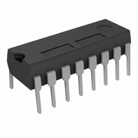
BU4021B Rohm Semiconductor, BU4021B Datasheet - Page 13

BU4021B
Manufacturer Part Number
BU4021B
Description
IC SHIFT REGISTER 8BIT 16DIP
Manufacturer
Rohm Semiconductor
Series
4000Br
Specifications of BU4021B
Logic Type
Shift Register
Output Type
Standard
Number Of Elements
1
Number Of Bits Per Element
8
Function
Parallel or Serial to Serial
Voltage - Supply
3 V ~ 16 V
Operating Temperature
-40°C ~ 85°C
Mounting Type
Through Hole
Package / Case
16-DIP (0.300", 7.62mm)
Lead Free Status / RoHS Status
Lead free / RoHS Compliant
Available stocks
Company
Part Number
Manufacturer
Quantity
Price
Company:
Part Number:
BU4021BF
Manufacturer:
MAXIM
Quantity:
118
Part Number:
BU4021BF
Manufacturer:
ROHM/罗姆
Quantity:
20 000
Part Number:
BU4021BF-T1
Manufacturer:
ROHM/罗姆
Quantity:
20 000
●Description of BU4021B series model
●Description of BU4094BC series model
© 2009 ROHM Co., Ltd. All rights reserved.
BU4015B,BU4015BF,BU4021B,BU4021BF,
BU4094BC,BU4094BCF,BU4094BCFV,BU4538B,BU4028B
www.rohm.com
Function: Dual 4-bit static shift register
VSS
Q6
Q8
P8
P4
P3
P2
P1
Function: 8-stage static shift register
1) Description of operation
PIN arrangement
Truth table
1) Description of operation
PIN arrangement
X:Don't Care
BU4021B is an 8-bit static shift register capable of parallel input/series output and series input/series output. In parallel
operation, DS (data) being asynchronous with the clock is inputted into each F/F and obtained at output.
In series operation, DS (data) is triggered by clock.
When P/S input level is “H”, parallel operation is effective, and when P/S input level is “L”, series operation is effective.
1
2
3
4
5
6
7
8
CLOCK
BU4094BC is an 8-stage shift/store register provided in each stage with a data latch with 3-state output. Data read into
shift register is read into the latch during the fall time of asynchronous STROBE input, and in the data transfer mode,
output can be held. Data is passed through the latch and outputted when the STROBE is in “H” level. Because the parallel
output becomes high impedance when the OUTPUT ENABLE terminal is set to “L” level by 3-state, the parallel output can
be connected directly with the 8-bit pass line.
X
STROBE
SERIAL
CLOCK
P8
Q6
Q8
P4
P3
P2
P1
IN
VSS
L
H
X
X
D
Q1
Q2
Q3
Q4
CLOCK
RESET
1
2
3
4
5
6
7
8
P/S
DS
Q5
Q7
P7
P6
L
L
L
H
Q0
STROBE
SERIA
Q1
Q2
Q3
Q4
L
H
L
16
15
14
13
12
11
10
CLOCK
9
IN
VDD
P7
P6
P5
Q7
DS
CLOCK
P/S
No Change
Q1
Q0
Q0
L
OUTPUT
ENABLE
CLOCK
P/S
Q2
Q1
Q1
Q'S
D
Q5
Q6
Q7
Q8
QS
L
Q3
Q2
Q2
L
Block diagram
D
P1
C
Q
16
15
14
13
12
11
10
9
P2
D
VDD
OUTPUT
ENABLE
Q5
Q6
Q7
Q8
Q'S
QS
X:Don't Care
*:Q6,Q7,Q8は外部
*:Q6,Q7,Q8:
C
Q
CLOCK
P3
D
C
Q
outside
P4
D
C
DS
Q
X
X
P5
D
13/17
C
P/S
Q
PIN description
H
H
PIN No.
P6
D
C
10
12
13
14
15
16
11
Q
Q
1
2
3
4
5
6
7
8
9
Dm
H
L
Q
P7
D
C
Q
Q
Qm*
H
Q
L
P8
D
SERIALIN
C Q
STROBE
ENABLE
Symbol
CLOCK
Q
VSS
VDD
Q’S
Q1
Q2
Q3
Q4
QS
Q8
Q7
Q6
Q5
PIN description
PIN No.
10
11
12
13
14
15
16
1
2
3
4
5
6
7
8
9
I/O
―
―
O
O
O
O
O
O
O
O
O
O
I
I
I
I
CLOCK
Symbol
VDD
VSS
P/S
DS
Q6
Q8
Q7
P8
P4
P3
P2
P1
P5
P6
P7
Parallel data output Q8
Parallel data output Q7
Parallel data output Q6
Parallel data output Q5
Serial data output Q’S
Parallel data input Q1
Parallel data input Q2
Parallel data input Q3
Parallel data input Q4
Serial data output QS
Power supply (+)
Power supply(-)
Output enable
Latch input
Clock input
Data input
I/O
―
―
Function
O
O
O
I
I
I
I
I
I
I
I
I
I
I
Technical Note
2009.06 - Rev.A
Parallel data input 8
Parallel data input 4
Parallel data input 3
Parallel data input 2
Parallel data input 1
Parallel data input 5
Parallel data input 6
Parallel data input 7
Power supply (+)
Serial data input
Power supply(-)
Parallel/Serial
Clock input
Function
Output 6
Output 8
Output 7


