BU4021B Rohm Semiconductor, BU4021B Datasheet - Page 14
BU4021B
Manufacturer Part Number
BU4021B
Description
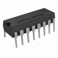
IC SHIFT REGISTER 8BIT 16DIP
Manufacturer
Rohm Semiconductor
Series
4000Br
Specifications of BU4021B
Logic Type
Shift Register
Output Type
Standard
Number Of Elements
1
Number Of Bits Per Element
8
Function
Parallel or Serial to Serial
Voltage - Supply
3 V ~ 16 V
Operating Temperature
-40°C ~ 85°C
Mounting Type
Through Hole
Package / Case
16-DIP (0.300", 7.62mm)
Lead Free Status / RoHS Status
Lead free / RoHS Compliant
Available stocks
Company
Part Number
Manufacturer
Quantity
Price
Company:

Part Number:
BU4021BF
Manufacturer:
MAXIM
Quantity:
118
Part Number:
BU4021BF
Manufacturer:
ROHM/罗姆
Quantity:
20 000
Part Number:
BU4021BF-T1
Manufacturer:
ROHM/罗姆
Quantity:
20 000


●Description of BU4538B series model
© 2009 ROHM Co., Ltd. All rights reserved.
BU4015B,BU4015BF,BU4021B,BU4021BF,
BU4094BC,BU4094BCF,BU4094BCFV,BU4538B,BU4028B
CDA
VSS
T1A
T2A
www.rohm.com
QA
QA
AA
BA
Block diagram
○ Switching characteristics
Function: Dual high accuracy monostable multivibrator
1) Description of operation
PIN arrangement
1
2
3
4
5
6
7
8
BU4538B is a re-triggerable monostable multi vibrator. Triggering is possible from either edge of the rise time and fall time
of input pulse. Output pulse setting is determined by the time constant (Rx · Cx) of external Rx and Cx.
Recommended output pulse amplitude is 200[μs]~1[s].
(Cautions on use: In case of system power down, etc., electric charge accumulated in the capacity Cx is discharged to the
VDD terminal through protective diode of 2 pins of 14 pins. When the electric current due to accumulated electric charge
exceeds 10[mA], IC may be destructed. When a large capacity Cx is used, electric current flowing into the IC can be
restricted by inserting the diode Dx.)
CD
CD
Q
Q
CHA
CHB
SERIAL IN
BA
BA
OUTPUT
ENABLE
CLOCK
STROBE
Q
Q
T1
T2
T1
T2
Truth table
Q1
PARALLEL OUTPUTS
16
15
14
13
12
11
10
9
SHIFT REGISTER
T1B
T2B
QB
X:Don't Care
CDB
AB
BB
QB
VDD
CLOCK
STROBE
OUTPUT
ENABLE
Q1 ~ Q7
QS
DATA
QS'
Q’S
OUTPUTS
8 STAGE
3 STATE
LACTH
8 BIT
H
L
X
A
DX
CX
tsu
CD
A
B
10%
INPUT
VDD
50%
RX
B
H
L
H
tPLH
50%
tWH
tTLH
Q8
Block diagram
th
90%
VDD
CD
H
H
H
H
L
90%
QS
Q'S
SERIAL
OUTPUT
Vref1
Enable
50%
tPHL
tTHL
50%
10%
Truth table
Q
L
L
L
Control
OUTPUT
S
Vref2
Q
tpLH
Enable
Reset Latch
50%
tWL
Q
H
H
H
tpLH
CLOCK
tPLH
Q
50%
50%
R
14/17
50%
90%
50%
OUTPUT
ENABLE
R
S
Output
Latch
tPHZ
H
H
H
H
L
H
Q
Q
STROBE
Q
Q
tPZH
H
H
X
X
H
L
10%
PIN description
PIN No. Symbol I/O
50%
SERIAL
10
11
12
13
14
15
16
1
2
3
4
5
6
7
8
9
IN
H
X
X
X
L
X
tPHL
50%
tPLZ
tpHL
50%
tr
10%
CDA
QAB
QBB
CCB
VDD
VSS
T1A
T2A
T2B
T1B
Parallel Output
NC
NC
10%
QA
QB
Q1
AA
BA
BB
AB
90%
H
L
Z
Z
tf
tPZL
90%
Qn-1
Qn-1
―
―
―
―
―
―
Qn
NC
O
O
O
O
NC
Z
Z
I
I
I
I
I
I
connection pin 1(CHA)
connection pin 2(CHA)
connection pin 1(CHB)
connection pin 2(CHB)
Passive component
Passive component
Passive component
Passive component
Reset input (CHA)
Reset input (CHB)
Qs
Q7
Q7
Q7
Q7
NC
NC
Serial Output
Output QB(CHA)
Output QB(CHB)
Power supply (+)
Technical Note
Power supply(-)
2009.06 - Rev.A
Output Q(CHA)
Output Q(CHB)
Input B(CHA)
Input B(CHB)
Input A(CHA)
Input A(CHB)
Function
Q's
NC
NC
NC
NC
Qs
Qs
Related parts for BU4021B
Image
Part Number
Description
Manufacturer
Datasheet
Request
R

Part Number:
Description:
Manufacturer:
Rohm Semiconductor
Datasheet:
Part Number:
Description:
Manufacturer:
Rohm Semiconductor
Datasheet:
Part Number:
Description:
Manufacturer:
Rohm Semiconductor
Datasheet:
Part Number:
Description:
Manufacturer:
Rohm Semiconductor
Datasheet:
Part Number:
Description:
Manufacturer:
Rohm Semiconductor
Datasheet:
Part Number:
Description:
Manufacturer:
Rohm Semiconductor
Datasheet:
Part Number:
Description:
Manufacturer:
Rohm Semiconductor
Datasheet:
Part Number:
Description:
Manufacturer:
Rohm Semiconductor
Datasheet:
Part Number:
Description:
Manufacturer:
Rohm Semiconductor
Datasheet:
Part Number:
Description:
Manufacturer:
Rohm Semiconductor
Datasheet:
Part Number:
Description:
Manufacturer:
Rohm Semiconductor
Datasheet:
Part Number:
Description:
Manufacturer:
Rohm Semiconductor
Datasheet:

Part Number:
Description:
DIODE SWITCH 80V 25MA SMD5 TR
Manufacturer:
Rohm Semiconductor
Datasheet: