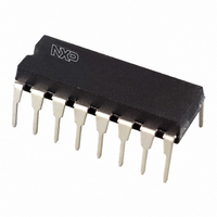
74HC257N,652 NXP Semiconductors, 74HC257N,652 Datasheet
74HC257N,652
Specifications of 74HC257N,652
74HC257N
933669550652


Related parts for 74HC257N,652


74HC257N,652 Summary of contents
Page 1
Quad 2-input multiplexer; 3-state Rev. 05 — 13 January 2010 1. General description The 74HC257; 74HCT257 are high-speed Si-gate CMOS devices and are pin compatible with Low-power Schottky TTL (LSTTL). The 74HC257 and 74HCT257 have four identical 2-input ...
Page 2
... NXP Semiconductors 3. Ordering information Table 1. Ordering information Type number Package Temperature range −40 °C to +125 °C 74HC257N 74HCT257N −40 °C to +125 °C 74HC257D 74HCT257D −40 °C to +125 °C 74HC257DB 74HCT257DB −40 °C to +125 °C 74HC257PW 74HCT257PW 4. Functional diagram mga835 Fig 1. Logic symbol ...
Page 3
... NXP Semiconductors 1 15 Fig 3. Functional diagram Fig 4. Logic diagram 74HC_HCT257_5 Product data sheet SELECTOR OE 3-STATE MULTIPLEXER OUTPUTS 1I0 1I1 2I0 2I1 3I0 3I1 4I0 4I1 OE S Rev. 05 — 13 January 2010 74HC257; 74HCT257 Quad 2-input multiplexer; 3-state mgr280 001aad468 © NXP B.V. 2010. All rights reserved. ...
Page 4
... NXP Semiconductors 5. Pinning information 5.1 Pinning Fig 5. Pin configuration DIP16, SO16, SSOP16 and TSSOP16 5.2 Pin description Table 2. Pin description Symbol Pin Description S 1 common data select input 1I0 to 4I0 2, 5, 11, 14 data input from source 0 1I1 to 4I1 3, 6, 10, 13 data input from source 1 ...
Page 5
... NXP Semiconductors 7. Limiting values Table 4. Limiting values In accordance with the Absolute Maximum Rating System (IEC 60134). Voltages are referenced to GND (ground = 0 V). Symbol Parameter V supply voltage CC I input clamping current IK I output clamping current OK I output current O I supply current CC I ground current ...
Page 6
... NXP Semiconductors 9. Static characteristics Table 6. Static characteristics At recommended operating conditions; voltages are referenced to GND (ground = 0 V). Symbol Parameter Conditions 74HC257 V HIGH-level input voltage LOW-level input voltage HIGH-level output voltage LOW-level output voltage input leakage current OFF-state output current supply current input capacitance ...
Page 7
... NXP Semiconductors Table 6. Static characteristics …continued At recommended operating conditions; voltages are referenced to GND (ground = 0 V). Symbol Parameter Conditions I OFF-state output current V O pin; other inputs at V GND supply current ΔI additional supply current other inputs per input pin; nI0, nI1 inputs per input pin ...
Page 8
... NXP Semiconductors Table 7. Dynamic characteristics Voltages are referenced to GND (ground = 0 V); For test circuit see Symbol Parameter Conditions t transition time see t C power dissipation per multiplexer; PD capacitance V I 74HCT257 t propagation delay nl0 nl1 to nY; pd see S to nY; see t enable time see ...
Page 9
... NXP Semiconductors 11. Waveforms S, nI0, nI1 Measurement points are given in V and V are typical voltage output levels that occur with the output load Fig 6. Propagation delays input (S, nI0, nI1) to output (nY) and output (nY) transition times OE input output LOW-to-OFF OFF-to-LOW output HIGH-to-OFF OFF-to-HIGH Measurement points are given in ...
Page 10
... NXP Semiconductors negative pulse positive pulse Measurement points are given in Definitions test circuit Termination resistance should be equal to output impedance Load capacitance including jig and probe capacitance Load resistor. L Fig 8. Test circuit for switching times Table 9. Test data Type Input 74HC257 74HCT257 ...
Page 11
... NXP Semiconductors 12. Package outline DIP16: plastic dual in-line package; 16 leads (300 mil pin 1 index 1 DIMENSIONS (inch dimensions are derived from the original mm dimensions UNIT b max. min. max. 1.73 mm 4.2 0.51 3.2 1.30 0.068 inches 0.17 0.02 0.13 0.051 Note 1. Plastic or metal protrusions of 0.25 mm (0.01 inch) maximum per side are not included. ...
Page 12
... NXP Semiconductors SO16: plastic small outline package; 16 leads; body width 3 pin 1 index 1 e DIMENSIONS (inch dimensions are derived from the original mm dimensions) A UNIT max. 0.25 1.45 mm 1.75 0.25 0.10 1.25 0.010 0.057 inches 0.069 0.01 0.004 0.049 Note 1. Plastic or metal protrusions of 0.15 mm (0.006 inch) maximum per side are not included. ...
Page 13
... NXP Semiconductors SSOP16: plastic shrink small outline package; 16 leads; body width 5 pin 1 index 1 e DIMENSIONS (mm are the original dimensions) A UNIT max. 0.21 1. 0.25 0.05 1.65 Note 1. Plastic or metal protrusions of 0.25 mm maximum per side are not included. OUTLINE VERSION IEC SOT338-1 Fig 11. Package outline SOT338-1 (SSOP16) ...
Page 14
... NXP Semiconductors TSSOP16: plastic thin shrink small outline package; 16 leads; body width 4 pin 1 index 1 e DIMENSIONS (mm are the original dimensions) A UNIT max. 0.15 0.95 mm 1.1 0.25 0.05 0.80 Notes 1. Plastic or metal protrusions of 0.15 mm maximum per side are not included. 2. Plastic interlead protrusions of 0.25 mm maximum per side are not included. ...
Page 15
... NXP Semiconductors 13. Revision history Table 10. Revision history Document ID Release date 74HC_HCT257_5 20100113 • Modifications: Table 7 “Dynamic 74HC_HCT257_4 20090608 74HC_HCT257_3 20050920 74HC_HCT257_CNV_2 19980930 74HC_HCT257_5 Product data sheet 74HC257; 74HCT257 Data sheet status Change notice Supersedes Product data sheet - characteristics”: changed 3OE to OE ...
Page 16
... Right to make changes — NXP Semiconductors reserves the right to make changes to information published in this document, including without limitation specifications and product descriptions, at any time and without notice ...
Page 17
... NXP Semiconductors 16. Contents 1 General description . . . . . . . . . . . . . . . . . . . . . . 1 2 Features . . . . . . . . . . . . . . . . . . . . . . . . . . . . . . . 1 3 Ordering information . . . . . . . . . . . . . . . . . . . . . 2 4 Functional diagram . . . . . . . . . . . . . . . . . . . . . . 2 5 Pinning information . . . . . . . . . . . . . . . . . . . . . . 4 5.1 Pinning . . . . . . . . . . . . . . . . . . . . . . . . . . . . . . . 4 5.2 Pin description . . . . . . . . . . . . . . . . . . . . . . . . . 4 6 Functional description . . . . . . . . . . . . . . . . . . . 4 6.1 Function table . . . . . . . . . . . . . . . . . . . . . . . . . . 4 7 Limiting values Recommended operating conditions Static characteristics Dynamic characteristics . . . . . . . . . . . . . . . . . . 7 11 Waveforms . . . . . . . . . . . . . . . . . . . . . . . . . . . . . 9 12 Package outline . . . . . . . . . . . . . . . . . . . . . . . . 11 13 Revision history ...