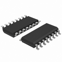
CBT3253AD,118 NXP Semiconductors, CBT3253AD,118 Datasheet - Page 5

CBT3253AD,118
Manufacturer Part Number
CBT3253AD,118
Description
IC 2BIT 1:4 FET MUX/DEMUX 16SOIC
Manufacturer
NXP Semiconductors
Series
74CBTr
Type
FET Multiplexer/Demuxr
Datasheet
1.CBT3253APW118.pdf
(17 pages)
Specifications of CBT3253AD,118
Circuit
2 x 1:4
Independent Circuits
1
Current - Output High, Low
15mA, 64mA
Voltage Supply Source
Single Supply
Voltage - Supply
4.5 V ~ 5.5 V
Operating Temperature
-40°C ~ 85°C
Mounting Type
Surface Mount
Package / Case
16-SOIC (3.9mm Width)
Lead Free Status / RoHS Status
Lead free / RoHS Compliant
Other names
935275884118
CBT3253AD-T
CBT3253AD-T
CBT3253AD-T
CBT3253AD-T
NXP Semiconductors
9. Static characteristics
Table 6.
T
[1]
[2]
[3]
10. Dynamic characteristics
Table 7.
V
[1]
[2]
[3]
CBT3253A_2
Product data sheet
Symbol
V
V
I
I
C
C
C
R
Symbol
t
t
t
LI
CC
PD
en
dis
amb
CC
I
IK
pass
i
io(off)
io(on)
on
CC
All typical values are at V
This is the increase in supply current for each input that is at the specified TTL voltage level rather than V
Measured by the voltage drop between the A and the B terminals at the indicated current through the switch. ON-state resistance is
determined by the lowest voltage of the two (A or B) terminals.
= +5.0 V
The propagation delay is the calculated RC time constant of the typical ON-state resistance of the switch and the specified load
capacitance, when driven by an ideal voltage source (zero output impedance).
Output enable time to HIGH and LOW level.
Output disable time from HIGH and LOW level.
= 40 C to +85 C
Parameter
propagation delay
enable time
disable time
Static characteristics
Dynamic characteristics
Parameter
input clamping voltage
pass voltage
input leakage current
quiescent supply current
additional quiescent supply
current (control inputs)
input capacitance
(control pins)
off-state input/output
capacitance
on-state input/output
capacitance
ON-state resistance
0.5 V; T
amb
[2]
[3]
CC
= 40 C to +85 C; unless otherwise specified.
= 5 V, T
Conditions
from input (nA or nBn) to output (nBn or nA)
from input (Sn) to output (nA or nBn)
from input (Sn) to output (nA or nBn)
from input (nOE) to output (nA or nBn)
from input (Sn) to output (nA or nBn)
from input (nOE) to output (nA or nBn)
[3]
amb
= 25 C.
Conditions
V
V
V
V
V
V
other inputs at V
V
A port; V
B port; V
A port and B port
V
V
V
CC
I
CC
CC
I
CC
I
CC
CC
CC
= V
= V
= 3 V or 0 V
= 4.5 V; I
= 5 V; V
= 5.5 V; I
= 5.5 V; one input at 3.4 V;
= 4.5 V; V
= 4.5 V; V
= 4.5 V; V
Rev. 02 — 8 February 2007
CC
CC
O
O
= 5.5 V; I
or GND
= 3 V or 0 V; OE = V
= 3 V or 0 V; OE = V
I
I
O
= 5.5 V or GND
I
I
I
= 18 mA
= 0 V; I
= 2.4 V; I
= 0 mA;
= 0 V; I
CC
O
or GND
= 100 A
I
I
= 30 mA
= 64 mA
I
= 15 mA
Dual 1-of-4 FET multiplexer/demultiplexer
CC
CC
[1]
[2]
Min
-
1.2
1.3
1.4
1.1
1.0
Min
-
3.4
-
-
-
-
-
-
-
-
-
-
Typ
-
-
-
-
-
-
Typ
-
3.6
-
-
-
4.5
11.4
3.8
18.6
5
5
10
CC
CBT3253A
or GND.
[1]
© NXP B.V. 2007. All rights reserved.
Max
0.25
6.2
6.3
6.4
7.2
7
Max
3.9
3
2.5
-
-
-
-
7
7
15
1.2
1
Unit
V
V
mA
pF
pF
pF
pF
Unit
ns
ns
ns
ns
ns
ns
A
A
5 of 17


