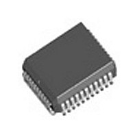
IDT728985J IDT, Integrated Device Technology Inc, IDT728985J Datasheet - Page 7

IDT728985J
Manufacturer Part Number
IDT728985J
Description
IC DGTL SW 256X256 44-PLCC
Manufacturer
IDT, Integrated Device Technology Inc
Series
7200r
Type
Multiplexerr
Datasheet
1.IDT728985JG.pdf
(13 pages)
Specifications of IDT728985J
Circuit
1 x 8:8
Independent Circuits
1
Voltage Supply Source
Single Supply
Voltage - Supply
4.75 V ~ 5.25 V
Operating Temperature
-40°C ~ 85°C
Mounting Type
Surface Mount
Package / Case
44-PLCC
Lead Free Status / RoHS Status
Contains lead / RoHS non-compliant
Current - Output High, Low
-
Lead Free Status / RoHS Status
Not Compliant, Contains lead / RoHS non-compliant
Other names
728985J
Available stocks
Company
Part Number
Manufacturer
Quantity
Price
Company:
Part Number:
IDT728985J
Manufacturer:
IDT, Integrated Device Technology Inc
Quantity:
10 000
Company:
Part Number:
IDT728985J8
Manufacturer:
IDT, Integrated Device Technology Inc
Quantity:
10 000
Company:
Part Number:
IDT728985JG
Manufacturer:
IDT, Integrated Device Technology Inc
Quantity:
10 000
Company:
Part Number:
IDT728985JG8
Manufacturer:
IDT, Integrated Device Technology Inc
Quantity:
10 000
NOTE:
1. If bit 2 of the corresponding Connection HIGH location is 1 or bit 6 of the Control Register is 1, then these entire 8 bits are output on the channel and stream associated with
IDT728985 Time Slot Interchange
Digital Switch 256 x 256
x = don't care
x = don't care
7,5,4,3
this location. Otherwise, the bits are used as indicated to define the source of the Connection which is output on the channel and stream associated with this location.
4-0
Bit
7-5
Bit
4-3
2-0
Bit
6
2
1
0
7
6
5
(1)
SAB2-0
(Source Stream Address Bits)
CAB2-0
(Source Channel Address Bits) is present is defined by bits SAB2-0). Bit 4 is the most significant bit.
SM (Split Memory)
PE (Processor Mode)
MS1-MS0
(Memory Select Bits)
STA2-0
(Stream Address Bits)
V/C (Variable/Constant
Throughput Delay Mode)
CS
(Channel Source)
OE (Output Enable)
CCO (CCO Bit)
(1)
(1)
Name
Name
Name
When 1, all subsequent reads are from the Data Memory and writes are to the Connection Memory, except when
the Control Register is accessed again. The Memory Select bits need to specify the memory for the operations.
When 1, the contents of the Connection Memory LOW are output on the Serial Output streams except when in high-
impedance. When 0, the Connection Memory bits for each channel determine what is output.
unused
0-0 - Not to be used.
0-1 - Data Memory (read only from the CPU)
1-0 - Connection Memory LOW
1-1 - Connection Memory is HIGH
The number expressed in binary notation on these bits refers to the input or output stream which corresponds to the
subsection of memory made accessible for subsequent operations.
unused
and stream. When 0, the contents of the corresponding location in Connection Memory LOW act as an address for the
This bit is used to select between Variable (LOW) and Constant Delay (HIGH) modes on a per-channel basis.
When 1, the contents of the corresponding location in Connection Memory LOW are output on the location's channel
Data Memory and determine the source of the connection to the location's channel and stream.
This bit drives a bit time on the CCO output pin.
This bit enables the output drivers on a per-channel basis. This allows individual channels on individual streams to
be made high-impedance, allowing switch matrices to be constructed. A HIGH enables the driver and a LOW disables it.
These three bits are used to select eight source streams for the Connection.
These five bits are used to select 32 different source channels for the Connection (the stream where the channel
SAB2
SM
X
7
7
7
SAB1
V/C
PE
6
6
6
SAB0
X
X
5
5
5
7
CAB4
MS1
X
4
4
4
CAB3
MS0
X
3
3
Description
Description
3
Description
STA2
CAB2
CS
2
2
2
STA1
CAB1
CCO
1
1
1
STA0
CAB0
OE
0
0
0
Commercial Temperature Range


