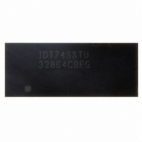
IDT74SSTU32864CBFG IDT, Integrated Device Technology Inc, IDT74SSTU32864CBFG Datasheet - Page 10

IDT74SSTU32864CBFG
Manufacturer Part Number
IDT74SSTU32864CBFG
Description
IC BUFFER REGISTER CONF 96-LFBGA
Manufacturer
IDT, Integrated Device Technology Inc
Datasheet
1.IDT74SSTU32864CBFG.pdf
(12 pages)
Specifications of IDT74SSTU32864CBFG
Logic Type
1:2 Configurable Registered Buffer
Supply Voltage
1.7 V ~ 1.9 V
Number Of Bits
25, 14
Operating Temperature
0°C ~ 70°C
Mounting Type
Surface Mount
Package / Case
96-LFBGA
Lead Free Status / RoHS Status
Lead free / RoHS Compliant
Other names
74SSTU32864CBFG
800-1693
800-1693
Available stocks
Company
Part Number
Manufacturer
Quantity
Price
Company:
Part Number:
IDT74SSTU32864CBFG
Manufacturer:
IDT
Quantity:
2 610
Company:
Part Number:
IDT74SSTU32864CBFG
Manufacturer:
IDT, Integrated Device Technology Inc
Quantity:
10 000
Part Number:
IDT74SSTU32864CBFG
Manufacturer:
IDT
Quantity:
20 000
Company:
Part Number:
IDT74SSTU32864CBFG8
Manufacturer:
IDT, Integrated Device Technology Inc
Quantity:
10 000
NOTES:
1. C
2. I
3. All input pulses are supplied by generators having the following characteristics: PRR ≤10MHz, Z
4. The outputs are measured one at a time with one transition per measurement.
5. V
6. V
7. V
8. V
9. t
TEST CIRCUITS AND WAVEFORMS (V
IDT74SSTU32864/A/C/D/G
1:1 AND 1:2 REGISTERED BUFFER WITH 1.8V SSTL I/O
LVCMOS
Input
Input
CLK
CLK
RESET
DD
PLH
I
TT
IH
IL
ID
DD
L
Input
includes probe and jig capacitance.
tested with clock and data inputs held at V
= V
= V
= 600mV.
= V
and t
REF
REF
REF
PHL
Voltage Waveforms - Setup and Hold Times
+ 250mV (AC voltage levels) for differential inputs. V
- 250mV (AC voltage levels) for differential inputs. V
= V
t
INACT
are the same as t
DD
Voltage Waveforms - Pulse Duration
/2
Inputs Active and Inactive Times
Voltage and Current Waveforms
V
CLK Inputs
DD
V
V
10%
ICR
REF
/2
t
SU
PDM
.
t
W
V
ICR
t
H
DD
R
Test Point
Test Point
or GND, and I
L =
T
L
100Ω
= 50Ω
V
DD
V
V
ICR
/2
REF
O
IL
IH
= 0mA
t
= GND for LVCMOS input.
ACT
= V
90%
V
0V
DD
V
DD
V
V
V
ID
CLK
CLK
ID
IH
IL
for LVCMOS input.
DUT
Load Circuit
DD
Out
10
= 1.8V ± 0.1V)
LVCMOS
Output
RESET
Output
CLK
CLK
Input
T
O
L
= 350ps, 50Ω
Voltage Waveforms - Propagation Delay Times
= 50Ω, input slew rate = 1 V/ns ±20% (unless otherwise specified).
Voltage Waveforms - Propagation Delay Times
C
L
t
PLH
= 30 pF
V
ICR
V
COMMERCIAL TEMPERATURE RANGE
TT
V
V
DD
DD
Test Point
/2
R
R
L
L
= 1KΩ
= 1KΩ
t
V
RPHL
V
ICR
TT
V
t
PHL
TT
V
V
V
ID
V
V
OH
OL
V
V
OH
OL
IH
IL


