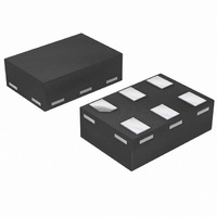
74AUP1Z125GM,115 NXP Semiconductors, 74AUP1Z125GM,115 Datasheet - Page 22

74AUP1Z125GM,115
Manufacturer Part Number
74AUP1Z125GM,115
Description
IC XTAL DRIVER LP 6-XSON
Manufacturer
NXP Semiconductors
Series
74AUPr
Datasheet
1.74AUP1Z125GW125.pdf
(32 pages)
Specifications of 74AUP1Z125GM,115
Logic Type
Inverter, X-Tal Driver
Supply Voltage
0.8 V ~ 3.6 V
Operating Temperature
-40°C ~ 125°C
Mounting Type
Surface Mount
Package / Case
*
Lead Free Status / RoHS Status
Lead free / RoHS Compliant
Number Of Bits
-
Lead Free Status / Rohs Status
Details
Other names
74AUP1Z125GM-G
74AUP1Z125GM-G
935280525115
74AUP1Z125GM-G
935280525115
NXP Semiconductors
74AUP1Z125
Product data sheet
13.1.1 Design
Figure 14
circuit is basically a Pierce oscillator circuit in which the crystal is operating at its
fundamental frequency and is tuned by the parallel load capacitance of C
C
drive-limiting resistor and is set to approximately the same value as the reactance of C
the crystal frequency (R
rail-to-rail output of X2. This keeps the drive level into the crystal within drive
specifications (the designer should verify this). Overdriving the crystal can cause damage.
The internal bias resistor provides negative feedback and sets a bias point of the inverter
near mid-supply, operating the 74AUP1GU04 in the high gain linear region.
To calculate the values of C
C
capacitance of the circuit (for the 74AUP1Z125 this is equal to an input capacitance
of 1.5 pF).
Fig 13. Reactance and resistance characteristics of a crystal
2
L
C
are in series with the crystal. They should be approximately equal. R
L
is the load capacitance as specified by the crystal manufacturer, C
=
(1) (a) = resonance
(2) (b) = anti-resonance
(3) (c) = load resonance
C
------------------ -
C
(1)
(2)
(3)
1
1
shows the recommended way to connect a crystal to the 74AUP1Z125. This
+
×
C
L
C
C
2
2
All information provided in this document is subject to legal disclaimers.
+
C
C
C
C
0
0
0
s
C
L
Low-power X-tal driver with enable and internal resistor; 3-state
Rev. 3 — 9 September 2010
1
= X
C
R
C
R
C
R
L
L
L
1
1
1
1
1
1
1
1
1
1
C1
and C
). This will result in an input to the crystal of 50 % of the
+
0
−
+
0
−
+
0
−
2
, the designer can use the formula:
R
1
R
L
f
r
f r
f
L
f
L
R
p
f
a
f
a
f
74AUP1Z125
a
resistance
resistance
resistance
reactance
reactance
reactance
s
is the stray
© NXP B.V. 2010. All rights reserved.
1
1
is the
and C
mnb104
f
f
f
∞
∞
∞
2
. C
22 of 32
1
and
1
at


