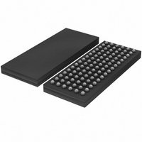
SSTU32866EC/G,557 NXP Semiconductors, SSTU32866EC/G,557 Datasheet - Page 12

SSTU32866EC/G,557
Manufacturer Part Number
SSTU32866EC/G,557
Description
IC BUFFER 1.8V 25BIT SOT536-1
Manufacturer
NXP Semiconductors
Datasheet
1.SSTU32866ECG551.pdf
(29 pages)
Specifications of SSTU32866EC/G,557
Logic Type
1:1, 1:2 Configurable Registered Buffer with Parity
Supply Voltage
1.7 V ~ 1.9 V
Number Of Bits
25, 14
Operating Temperature
0°C ~ 70°C
Mounting Type
Surface Mount
Package / Case
96-LFBGA
Logic Family
SSTU
Logical Function
Registered Buffer
Number Of Elements
1
Number Of Inputs
25
Number Of Outputs
25
High Level Output Current
-8mA
Low Level Output Current
8mA
Propagation Delay Time
3ns
Operating Supply Voltage (typ)
1.8V
Operating Supply Voltage (max)
1.9V
Operating Supply Voltage (min)
1.7V
Clock-edge Trigger Type
Posit/Negat-Edge
Polarity
Non-Inverting
Technology
CMOS
Frequency (max)
450(Min)MHz
Mounting
Surface Mount
Pin Count
96
Operating Temp Range
0C to 70C
Operating Temperature Classification
Commercial
Lead Free Status / RoHS Status
Lead free / RoHS Compliant
Other names
935275473557
SSTU32866EC/G
SSTU32866EC/G
SSTU32866EC/G
SSTU32866EC/G
Philips Semiconductors
Table 6:
[1]
[2]
10. Characteristics
Table 7:
At recommended operating conditions (see
9397 750 14181
Product data sheet
Symbol
V
I
I
T
Symbol
V
V
I
I
I
C
OH
OL
I
DD
DDD
amb
ID
OH
OL
i
The RESET and Cn inputs of the device must be held at valid levels (not floating) to ensure proper device operation.
The differential inputs must not be floating, unless RESET is LOW.
Recommended operating conditions
Characteristics
Parameter
HIGH-level output voltage
LOW-level output voltage
input current
static standby current
static operating current
dynamic operating current per MHz,
clock only
dynamic operating current per MHz,
per each data input, 1:1 mode
dynamic operating current per MHz,
per each data input, 1:2 mode
input capacitance, data and CSR
inputs
input capacitance,
CK and CK inputs
input capacitance, RESET input
Parameter
differential input voltage
HIGH-level output current
LOW-level output current
operating ambient temperature
in free air
Table
Conditions
CK, CK
Rev. 02 — 11 November 2004
Conditions
I
I
all inputs; V
V
RESET = GND; I
V
RESET = V
V
RESET = V
V
switching at 50 % duty cycle.
I
RESET = V
V
switching at 50 % duty cycle. One
data input switching at half clock
frequency, 50 % duty cycle.
I
RESET = V
V
switching at 50 % duty cycle. One
data input switching at half clock
frequency, 50 % duty cycle.
I
V
V
V
V
6), unless otherwise specified.
OH
OL
O
O
O
DD
DD
DD
I
I
I
I
ICR
DD
I
…continued
= V
= 0 mA; V
= V
= 0 mA; V
= V
= 0 mA; V
= V
= V
= 6 mA; V
= 6 mA; V
= 1.9 V
= 1.9 V
= 1.9 V; V
= 1.8 V
= 0.9 V; V
IH(AC)
IH(AC)
IH(AC)
REF
DD
or GND; V
DD
DD
DD
DD
I
1.8 V DDR2 configurable registered buffer with parity
or V
or V
or V
250 mV; V
DD
DD
DD
= V
DD
; I
;
;
;
I
[2]
i(p-p)
DD
= V
= 1.8 V
= 1.8 V
= 1.8 V
O
IL(AC)
IL(AC)
IL(AC)
DD
= 1.7 V
O
= 0 mA;
Min
600
-
-
0
= 1.7 V
= 0 mA;
IH(AC)
or GND;
= 600 mV;
DD
; CK and CK
; CK and CK
; CK and CK
DD
= 1.8 V
or V
= 1.8 V
IL(AC)
Typ
-
-
-
-
© Koninklijke Philips Electronics N.V. 2004. All rights reserved.
Min
1.2
-
-
-
-
-
-
-
2.5
2
3
SSTU32866
Max
-
8
+70
Typ
-
-
-
-
-
16
11
19
-
-
-
8
Max
-
0.5
100
40
-
-
-
3.5
3
4
5
12 of 29
Unit
V
V
mA
pF
pF
pF
Unit
mV
mA
mA
A
A
A
A
A
C


