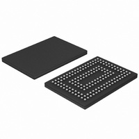
SSTU32865ET/G,551 NXP Semiconductors, SSTU32865ET/G,551 Datasheet - Page 27

SSTU32865ET/G,551
Manufacturer Part Number
SSTU32865ET/G,551
Description
IC REG BUFFER 28BIT 160-TFBGA
Manufacturer
NXP Semiconductors
Datasheet
1.SSTU32865ETG518.pdf
(29 pages)
Specifications of SSTU32865ET/G,551
Logic Type
1:2 Registered Buffer with Parity
Supply Voltage
1.7 V ~ 1.9 V
Number Of Bits
28
Operating Temperature
0°C ~ 70°C
Mounting Type
Surface Mount
Package / Case
160-TFBGA
Lead Free Status / RoHS Status
Lead free / RoHS Compliant
Other names
935275433551
SSTU32865ET/G-S
SSTU32865ET/G-S
SSTU32865ET/G-S
SSTU32865ET/G-S
Available stocks
Company
Part Number
Manufacturer
Quantity
Price
Company:
Part Number:
SSTU32865ET/G,551
Manufacturer:
NXP Semiconductors
Quantity:
10 000
Philips Semiconductors
14. Revision history
Table 13:
9397 750 13799
Product data sheet
Document ID
SSTU32865_2
Modifications:
SSTU32865-01
Revision history
Release date
20040928
20040705
•
•
•
•
•
•
•
•
•
•
•
•
•
•
•
The format of this data sheet has been redesigned to comply with the new presentation and
information standard of Philips Semiconductors.
Section 1 “General
Section 2
Additional features added to
Section 6 “Pinning information”
– change ‘MCL’ to ‘m.c.l.’ and ‘MCH’ to ‘m.c.h.’
– add descriptions for VDDL and VDDR in
– added
– added
Table 3 “Function table (each flip-flop)”
Section 7.1 on page
Table 3 “Function table (each
Table 4 “Parity and standby function
–
– Add
Section 7.3.4 “Power-up
Table 6 “Limiting
– Symbol V
– Symbols ESD
Table 7 “Recommended operating
– change V
– change V
– Table note split into 2 notes; references added.
Table 8 “Characteristics”
– change I
– change Typical value for I
– change Typical value for I
Table 9 “Timing
– change symbol f
– change f
– change symbol t
– change symbol t
Table 10 “Switching
– change f
– change t
– change t
Section 11.1 “Test
Table note
MHz ...”; change Unit from “ A/MHz” to “ A”.
Table note
“Features”: acronym SSTL defined.
Figure 2 “Pin configuration for TFBGA160”
Figure 3 “Ball mapping”
Data sheet status
Product data sheet
Product data
DDD
clock
MAX
PDM
PDMSS
IH
IL
i
changed to V
2: change ‘This transition assumes ...’ to ‘This condition assumes ...’.
(for data inputs) to V
(for data inputs) to V
Parameter from “dynamic operating current ...” to “dynamic operating current per
requirements”:
minimum value from 270 MHz to 450 MHz
maximum value from 2.15 ns to 1.8 ns
maximum value from 270 MHz to 450 MHz
values”:
HBM
maximum value from 2.35 ns to 2.0 ns
circuit”: acronym PRR defined; titles for
3.
description”: acronym TFBGA defined.
CLOCK
SU
H
characteristics”:
Rev. 02 — 28 September 2004
8.
and ESD
to t
to t
sequence”: add ‘(HIGH)’ after ‘... and will be held clear’.
h
su
to f
I
; under ‘Conditions’, change ‘Chip Select’ to ‘DCS0, DCS1’.
; Symbol V
Section 2 “Features”
DDD
DDD
clock
flip-flop)”: add
MM
(clock only) from TBD to 16 A
(per each data input) from TBD to 19 A
replaced with V
(replaces Table 2 “Ball mapping”)
conditions”:
IL(AC)
IH(AC)
table”:
Change notice
-
-
o
and
changed to V
and V
and V
Table 4 “Parity and standby function table”
Table 2 “Pin description”
Table note 1
IL(DC)
IH(DC)
esd
1.8 V DDR registered buffer with parity
; condition changed to ‘data inputs (Dn)
; condition changed to ‘data inputs (Dn)’
(added model types under “Conditions”)
O
.
Doc. number
9397 750 13799
9397 750 10942
and its reference at ‘Outputs’.
Figure 12
© Koninklijke Philips Electronics N.V. 2004. All rights reserved.
and
SSTU32865
Figure 13
Supersedes
SSTU32865-01
-
modified.
moved to
27 of 29


