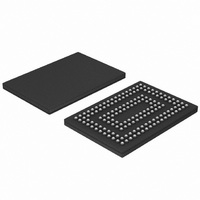
SSTUG32865ET/S,518 NXP Semiconductors, SSTUG32865ET/S,518 Datasheet - Page 7

SSTUG32865ET/S,518
Manufacturer Part Number
SSTUG32865ET/S,518
Description
IC BUFFER 1.8V 28BIT 160-TFBGA
Manufacturer
NXP Semiconductors
Datasheet
1.SSTUG32865ETG518.pdf
(28 pages)
Specifications of SSTUG32865ET/S,518
Logic Type
1:2 Registered Buffer with Parity
Supply Voltage
1.7 V ~ 2 V
Number Of Bits
28
Operating Temperature
0°C ~ 85°C
Mounting Type
Surface Mount
Package / Case
160-TFBGA
Lead Free Status / RoHS Status
Lead free / RoHS Compliant
Other names
935284904518
SSTUG32865ET/S-T
SSTUG32865ET/S-T
SSTUG32865ET/S-T
SSTUG32865ET/S-T
Available stocks
Company
Part Number
Manufacturer
Quantity
Price
Company:
Part Number:
SSTUG32865ET/S,518
Manufacturer:
NXP Semiconductors
Quantity:
10 000
NXP Semiconductors
Table 3.
[1]
SSTUG32865_1
Product data sheet
Symbol
Program inputs
CSGATEEN
SELDR
Clock inputs
CK, CK
Miscellaneous inputs
MCL
MCH
RESET
VREF
VDDL
VDDR
GND
n.c.
If application does not require DCS2 and DCS3, it is allowed to connect H4 and K4 to V
Pin description
Pin
H1
A2
J1, K1
U3, V2, V3
U5, V5
L1
A1, V1
D4, E4, E6, F4, G4, K5, N4,
N5, P5, P6, R5, R6
E7, F8, F9, G8, G9, J8, J9,
L8, L9, N8, N9, P7, P8
D5, D8, D9, E5, E8, E9, F5,
G5, H5, H8, H9, J4, J5, K8,
K9, L4, L5, M4, M5, M8, M9,
P4, P9, R4, R7, R8, R9
A4, A5, B3, B4, B5, D6, D7,
V4
…continued
Rev. 01 — 16 August 2007
Type
1.8 V
LVCMOS
with weak
pull-up
LVCMOS
input
SSTL_18
1.8 V
LVCMOS
with weak
pull-up
0.9 V
nominal
Description
Chip Select Gate Enable. When HIGH, the D0 to D21
inputs will be latched only when at least one Chip Select
input is LOW during the rising edge of the clock. When
LOW, the D0 to D21 inputs will be latched and redriven
on every rising edge of the clock.
Selects output drive strength: ‘HIGH’ for normal drive,
‘LOW’ for high drive. This pin will default HIGH if left
open-circuit (built-in weak pull-up resistor).
Differential master clock input pair to the register. The
register operation is triggered by a rising edge on the
positive clock input (CK).
Must be connected to a logic LOW.
Must be connected to a logic HIGH.
Asynchronous reset input. When LOW, it causes a reset
of the internal latches, thereby forcing the outputs LOW.
RESET also resets the PTYERR signal.
Input reference voltage for the SSTL_18 inputs. Two pins
(internally tied together) are used for increased reliability.
Power supply voltage.
Power supply voltage.
Ground.
Ball present but not connected to die.
1.8 V DDR2-1G registered buffer with parity
DD
.
SSTUG32865
© NXP B.V. 2007. All rights reserved.
7 of 28


