SSTVA16857AG IDT, Integrated Device Technology Inc, SSTVA16857AG Datasheet
SSTVA16857AG
Specifications of SSTVA16857AG
Available stocks


Related parts for SSTVA16857AG


SSTVA16857AG Summary of contents
Page 1
Integrated Circuit Systems, Inc. DDR 14-Bit Registered Buffer Recommended Applications: • DDR Memory Modules • Provides complete DDR DIMM logic solution with ICS93V857 or ICS95V857 • SSTL_2 compatible data registers • DDR400 recommended (backward compatible to DDR200/266/333) Product Features: • ...
Page 2
ICSSSTVA16857 General Description The 14-bit ICSSSTVA16857 is a universal bus driver designed for 2.3V to 2.7V V except for the LVCMOS RESET# input. Data flow from controlled by the differential clock (CLK/CLK#) and a control signal ...
Page 3
Absolute Maximum Ratings Storage Temperature . . . . . . . . . . . . . . . . . . . . –65°C to +150°C Supply Voltage . . . . . . . . . . ...
Page 4
ICSSSTVA16857 Recommended Operating Conditions - DDRI-400 (PC3200) DESCRIPTION PARAMETER Supply Voltage V DD I/O Supply Voltage V DDQ Reference Voltage V REF Termination Voltage Input Voltage Input High Voltage IH (DC Input ...
Page 5
DC Electrical Characteristics - DDRI/DDR333 (PC1600, PC2100, PC2700 70° 2.5 +/-0.2V DDQ SYMBOL PARAMETERS -18mA ...
Page 6
ICSSSTVA16857 DC Electrical Characteristics - DDRI-400 (PC3200 70° 2.5 +/-0.2V DDQ SYMBOL PARAMETERS -18mA ...
Page 7
Timing Requirements (over recommended operating free-air temperature range, unless otherwise noted) SYMBOL PARAMETERS f Clock frequency clock t Output slew rate SL Setup time, fast slew rate t S Setup time, slow slew rate Hold time, fast slew rate ...
Page 8
ICSSSTVA16857 LVCMOS RESET DDQ Input t inact I DD (see note 2) 10% Voltage and Current Waveforms Inputs Active and Inactive Times t w Input V REF Voltage Waveforms - Pulse Duration Timing Input Input ...
Page 9
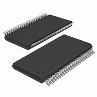
INDEX INDEX AREA AREA aaa 6.10 mm. Body, 0.50 mm. pitch TSSOP (0.020 mil) (240 mil) Ordering Information ICSSSTVA16857yGLF-T Example: ICS XXXX y G LF- T Designation ...