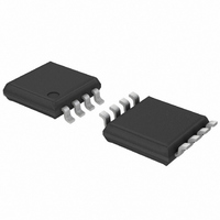
74AVC2T45DP,125 NXP Semiconductors, 74AVC2T45DP,125 Datasheet - Page 9

74AVC2T45DP,125
Manufacturer Part Number
74AVC2T45DP,125
Description
IC BUS TRANSCVR TRI-ST DL 8TSSOP
Manufacturer
NXP Semiconductors
Series
74AVCr
Datasheet
1.74AVC2T45DP125.pdf
(27 pages)
Specifications of 74AVC2T45DP,125
Package / Case
8-TSSOP
Logic Function
Translator, Bidirectional, 3-State
Number Of Bits
2
Input Type
Logic
Output Type
Logic
Number Of Channels
2
Number Of Outputs/channel
1
Differential - Input:output
No/No
Propagation Delay (max)
2.4ns
Voltage - Supply
0.8 V ~ 3.6 V
Operating Temperature
-40°C ~ 125°C
Supply Voltage
0.8 V ~ 3.6 V
Mounting Style
SMD/SMT
Data Rate
-
Lead Free Status / RoHS Status
Lead free / RoHS Compliant
Data Rate
-
Lead Free Status / Rohs Status
Lead free / RoHS Compliant
Other names
74AVC2T45DP-G
74AVC2T45DP-G
935286774125
74AVC2T45DP-G
935286774125
NXP Semiconductors
11. Dynamic characteristics
Table 9.
Voltages are referenced to GND (ground = 0 V); for test circuit see
[1]
Table 10.
Voltages are referenced to GND (ground = 0 V); for test circuit see
[1]
Table 11.
Voltages are referenced to GND (ground = 0 V).
[1]
[2]
74AVC2T45
Product data sheet
Symbol Parameter
t
t
t
Symbol Parameter
t
t
t
Symbol Parameter
C
pd
dis
en
pd
dis
en
PD
t
t
t
t
C
P
f
f
C
V
N = number of inputs switching;
Σ(C
f
pd
en
pd
en
i
o
i
D
CC
PD
= input frequency in MHz;
L
= 10 MHz; V
= output frequency in MHz;
is the same as t
is a calculated value using the formula shown in
is the same as t
is a calculated value using the formula shown in
= load capacitance in pF;
= C
L
is used to determine the dynamic power dissipation (P
= supply voltage in V;
× V
propagation delay A to B
disable time
enable time
propagation delay A to B
disable time
enable time
power dissipation
capacitance
PD
Typical dynamic characteristics at V
Typical dynamic characteristics at V
Typical power dissipation capacitance at V
CC
× V
2
× f
CC
I
o
= GND to V
2
) = sum of the outputs.
× f
PLH
PLH
i
× N + Σ(C
and t
and t
CC
PHL
PHL
; t
Conditions
B to A
DIR to A
DIR to B
DIR to A
DIR to B
Conditions
B to A
DIR to A
DIR to B
DIR to A
DIR to B
Conditions
A port: (direction A to B);
B port: (direction B to A)
A port: (direction B to A);
B port: (direction A to B)
L
; t
; t
r
× V
= t
dis
dis
f
CC
is the same as t
is the same as t
= 1 ns; C
2
× f
o
All information provided in this document is subject to legal disclaimers.
) where:
L
= 0 pF; R
Dual-bit, dual-supply voltage level translator/transceiver; 3-state
Rev. 5 — 30 November 2010
Section 13.4 “Enable times”
Section 13.4 “Enable times”
PLZ
PLZ
CC(A)
CC(B)
and t
and t
L
= ∞ Ω.
= 0.8 V and T
= 0.8 V and T
D
CC(A)
PHZ
PHZ
in μW).
0.8 V
0.8 V
0.8 V
15.5
15.5
12.2
11.7
27.2
27.7
15.5
15.5
12.2
11.7
27.2
27.7
1
9
; t
; t
en
en
= V
is the same as t
is the same as t
CC(B)
Figure
Figure
1.2 V
1.2 V
1.2 V
12.7
12.2
20.6
20.3
17.3
17.6
12.7
amb
8.1
7.9
amb
8.1
4.9
9.2
11
2
and T
8; for wave forms see
8; for wave forms see
= 25 °C
= 25 °C
amb
V
PZL
PZL
1.5 V
1.5 V
1.5 V
CC(A)
12.3
12.2
19.9
19.8
12.3
16.6
16.1
7.6
7.6
7.6
3.8
9.0
11
2
= 25 °C
[1]
[1]
and t
and t
V
V
and V
CC(B)
CC(A)
PZH
PZH
1.8 V
1.8 V
1.8 V
12.2
12.2
20.4
19.9
.
12.2
16.5
15.9
.
[1][2]
7.7
8.2
7.7
3.7
8.8
12
CC(B)
2
Figure 6
Figure 6
74AVC2T45
2.5 V
2.5 V
2.5 V
12.0
12.2
20.7
20.6
12.0
17.1
14.8
8.4
8.7
8.4
2.8
8.7
14
2
© NXP B.V. 2010. All rights reserved.
and
and
Figure 7
Figure 7
3.3 V
3.3 V
3.3 V
12.2
10.2
22.0
21.4
17.8
15.2
11.8
11.8
9.2
9.2
3.4
8.6
17
2
9 of 27
Unit
ns
ns
ns
ns
ns
ns
Unit
ns
ns
ns
ns
ns
Unit
pF
pF
ns


