74ALVC162334ADGG:5 NXP Semiconductors, 74ALVC162334ADGG:5 Datasheet
74ALVC162334ADGG:5
Specifications of 74ALVC162334ADGG:5
74ALVC162334ADG-T
935267301518


Related parts for 74ALVC162334ADGG:5


74ALVC162334ADGG:5 Summary of contents
Page 1
Rev. 03 — 13 December 2006 1. General description The 74ALVC162334A is a 16-bit universal bus driver. Data flow is controlled by active LOW output enable (OE), ...
Page 2
... NXP Semiconductors 3. Quick reference data Table 1. Quick reference data V = 3.3 V 0.3 V; GND = Symbol Parameter t HIGH-to-LOW propagation delay PHL t LOW-to-HIGH propagation delay PLH f maximum input clock frequency max C input capacitance i C input/output capacitance io C power dissipation capacitance PD [1] All typical values are ...
Page 3
... NXP Semiconductors 5. Functional diagram Fig 1. Logic symbol (IEEE/IEC) Fig 2. Logic diagram Fig 3. Typical input (data or control) 74ALVC162334A_3 Product data sheet 1 OE EN1 48 CP 2C3 Y10 16 Y11 17 Y12 19 Y13 20 Y14 22 Y15 23 Y16 002aac723 the 15 other channels 002aac725 Rev. 03 — 13 December 2006 74ALVC162334A ...
Page 4
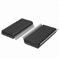
... NXP Semiconductors 6. Pinning information 6.1 Pinning Fig 4. Pin configuration for TSSOP48 6.2 Pin description Table 3. Symbol GND 74ALVC162334A_3 Product data sheet GND GND 74ALVC162334ADGG Y9 13 Y10 14 15 GND Y11 16 Y12 Y13 Y14 20 GND 21 22 Y15 23 Y16 n.c. 24 Pin description Pin ...
Page 5
... NXP Semiconductors Table 3. Symbol Y9 Y10 Y11 Y12 Y13 Y14 Y15 Y16 n.c. LE A16 A15 A14 A13 A12 A11 A10 74ALVC162334A_3 Product data sheet Pin description …continued Pin Description 13 data output 9 14 data output 10 16 data output 11 17 data output 12 19 data output 13 ...
Page 6
... NXP Semiconductors 7. Functional description Refer to 7.1 Function selection Table HIGH voltage level LOW voltage level Don’t care high-impedance OFF-state; = LOW to HIGH level transition. Inputs [1] Output level before the indicated steady-state input conditions were established, provided that CP is HIGH before LE goes LOW. ...
Page 7
... NXP Semiconductors 8. Limiting values Table 5. Limiting values In accordance with the Absolute Maximum Rating System (IEC 60134). Voltages are referenced to GND (ground = 0 V). Symbol Parameter V supply voltage CC I input clamping current IK V input voltage I I output clamping current OK V output voltage O I output sink or source current ...
Page 8
... NXP Semiconductors 10. Static characteristics Table 7. Static characteristics +85 C; over recommended operating conditions; voltages are referenced to GND (ground = 0 V); amb unless otherwise specified. Symbol Parameter V HIGH-level input voltage IH V LOW-level input voltage IL V HIGH-level output voltage LOW-level output voltage OL I input leakage current ...
Page 9
... NXP Semiconductors C = output load capacitance in pF output frequency in MHz supply voltage sum of outputs 11. Dynamic characteristics Table 8. Dynamic characteristics for 2 2.7 V; GND = Symbol Parameter t HIGH-to-LOW propagation delay PHL t LOW-to-HIGH propagation delay PLH t OFF-state to HIGH propagation delay OE to Yn; PZH t OFF-state to LOW propagation delay OE to Yn; ...
Page 10
... NXP Semiconductors Table 9. Dynamic characteristics for 2.7 V; GND = 2.5 ns Symbol Parameter t pulse width w t set-up time su t hold time h f maximum input clock frequency max [1] All typical values are measured at T [2] 3-state output enable time. [3] 3-state output disable time. Table 10. ...
Page 11
... NXP Semiconductors 11.1 AC waveforms 3.6 V and 1 2 2.7 V and 0 input PHL Yn output V M Fig 5. Input (An) to output (Yn) propagation delay input input The shaded areas indicate when the input is permitted to change for predictable output performance. Fig 7. Data set-up and hold times, An input to ...
Page 12
... NXP Semiconductors 12. Test information Fig 11. Test circuitry for switching times Table 11. Supply voltage 2.7 V 2 3.6 V 74ALVC162334A_3 Product data sheet V I PULSE GENERATOR Test data are given in Table 11 load resistance load capacitance includes jig and probe capacitance termination resistance should be equal to Z ...
Page 13
... NXP Semiconductors 13. Package outline TSSOP48: plastic thin shrink small outline package; 48 leads; body width 6 pin 1 index 1 DIMENSIONS (mm are the original dimensions). A UNIT max. 0.15 1.05 mm 1.2 0.25 0.05 0.85 Notes 1. Plastic or metal protrusions of 0.15 mm maximum per side are not included. 2. Plastic interlead protrusions of 0.25 mm maximum per side are not included. ...
Page 14
... NXP Semiconductors 14. Soldering This text provides a very brief insight into a complex technology. A more in-depth account of soldering ICs can be found in Application Note AN10365 “Surface mount reflow soldering description” . 14.1 Introduction to soldering Soldering is one of the most common methods through which packages are attached to Printed Circuit Boards (PCBs), to form electrical circuits ...
Page 15
... NXP Semiconductors 14.4 Reflow soldering Key characteristics in reflow soldering are: • Lead-free versus SnPb soldering; note that a lead-free reflow process usually leads to higher minimum peak temperatures (see reducing the process window • Solder paste printing issues including smearing, release, and adjusting the process window for a mix of large and small components on one board • ...
Page 16
... Release date 74ALVC162334A_3 20061213 • Modifications: The format of this data sheet has been redesigned to comply with the new identity guidelines of NXP Semiconductors. • Legal texts have been adapted to the new company name where appropriate. • Section 1 “General • Table 2 “Ordering TSSOP48) package • ...
Page 17
... NXP Semiconductors Table 15. Revision history …continued Document ID Release date • Modifications: Figure 1 “Logic symbol (continued) • Figure 2 “Logic – changed signal “A – changed signal “Y – changed “to the 17 other channels” to “to the 15 other channels” • Table 5 “Limiting values” ...
Page 18
... For detailed and full information see the relevant full data sheet, which is available on request via the local NXP Semiconductors sales office. In case of any inconsistency or conflict with the short data sheet, the full data sheet shall prevail ...
Page 19
... NXP Semiconductors 19. Contents 1 General description . . . . . . . . . . . . . . . . . . . . . . 1 2 Features . . . . . . . . . . . . . . . . . . . . . . . . . . . . . . . 1 3 Quick reference data . . . . . . . . . . . . . . . . . . . . . 2 4 Ordering information . . . . . . . . . . . . . . . . . . . . . 2 5 Functional diagram . . . . . . . . . . . . . . . . . . . . . . 3 6 Pinning information . . . . . . . . . . . . . . . . . . . . . . 4 6.1 Pinning . . . . . . . . . . . . . . . . . . . . . . . . . . . . . . . 4 6.2 Pin description . . . . . . . . . . . . . . . . . . . . . . . . . 4 7 Functional description . . . . . . . . . . . . . . . . . . . 6 7.1 Function selection Limiting values Recommended operating conditions Static characteristics Dynamic characteristics . . . . . . . . . . . . . . . . . . 9 11.1 AC waveforms ...