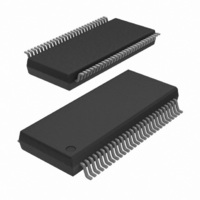
74LVT16500ADL,518 NXP Semiconductors, 74LVT16500ADL,518 Datasheet
74LVT16500ADL,518
Specifications of 74LVT16500ADL,518
74LVT16500ADL-T
935194780518


Related parts for 74LVT16500ADL,518


74LVT16500ADL,518 Summary of contents
Page 1
V 18-bit universal bus transceiver; 3-state Rev. 03 — 29 May 2006 1. General description The 74LVT16500A is a high-performance BiCMOS product designed for V 3.3 V. This device is an 18-bit universal transceiver featuring non-inverting 3-state bus ...
Page 2
Philips Semiconductors 3. Ordering information Table 1. Ordering information Type number Package Temperature range Name 74LVT16500ADGG +85 C 74LVT16500ADL + Functional diagram ...
Page 3
Philips Semiconductors Fig 3. Logic diagram 74LVT16500A_3 Product data sheet 3.3 V 18-bit universal bus transceiver; 3-state 1 OEAB 55 CPAB 2 LEAB 28 LEBA 30 CPBA 27 OEBA CLK to 17 other channels Rev. 03 ...
Page 4
Philips Semiconductors 5. Pinning information 5.1 Pinning Fig 4. Pin configuration 5.2 Pin description Table 2. Symbol OEAB LEAB A0 GND 74LVT16500A_3 Product data sheet 3.3 V 18-bit universal bus transceiver; 3-state 74LVT16500A 1 OEAB 2 ...
Page 5
Philips Semiconductors Table 2. Symbol GND A10 A11 GND A12 A13 A14 V CC A15 A16 GND A17 OEBA LEBA GND CPBA B17 GND B16 B15 V CC B14 B13 B12 GND B11 ...
Page 6
Philips Semiconductors Table 2. Symbol GND B0 CPAB GND 6. Functional description Table 3. Operating mode disabled disabled, latch data disabled, latch data disabled, hold data disabled, clock data disabled, clock data transparent transparent latch ...
Page 7
Philips Semiconductors 7. Limiting values Table 4. In accordance with the Absolute Maximum Rating System (IEC 60134). Voltages are referenced to GND (ground = 0 V). Symbol Parameter ...
Page 8
Philips Semiconductors 9. Static characteristics Table 6. Static characteristics At recommended operating conditions; voltages are referenced to GND (ground = 0 V). Symbol Parameter [ amb V input clamping voltage IK V HIGH-level ...
Page 9
Philips Semiconductors Table 6. Static characteristics At recommended operating conditions; voltages are referenced to GND (ground = 0 V). Symbol Parameter I additional quiescent supply CC current C input capacitance i C input/output capacitance io [1] Typical values are at ...
Page 10
Philips Semiconductors Table 7. Dynamic characteristics Voltages are referenced to GND (ground = 0 V); for test circuit see Symbol Parameter t setup time LOW su( CPAB CPBA An to LEAB with CPAB LOW or ...
Page 11
Philips Semiconductors Table 7. Dynamic characteristics Voltages are referenced to GND (ground = 0 V); for test circuit see Symbol Parameter t hold time HIGH h( CPAB CPBA An to LEAB LEBA ...
Page 12
Philips Semiconductors Fig 6. Propagation delay clock (CPAB, CPBA) to output (An, Bn), clock (CPAB, CPBA) Fig 7. Propagation delay latch enable (LEAB, LEBA) to output (An, Bn) and latch enable Fig 8. 3-state output enable time to HIGH-level and ...
Page 13
Philips Semiconductors Fig 9. 3-state output enable time to LOW-level and output disable time from LOW-level Fig 10. Data setup and hold times Table 8. Supply voltage 2.7 V 3.3 V 74LVT16500A_3 Product data sheet OEBA V I input 0 ...
Page 14
Philips Semiconductors Fig 11. Load circuitry for switching times Table 9. Input V I 2.7 V 74LVT16500A_3 Product data sheet negative V M pulse ...
Page 15
Philips Semiconductors 12. Package outline TSSOP56: plastic thin shrink small outline package; 56 leads; body width 6 pin 1 index 1 DIMENSIONS (mm are the original dimensions). A UNIT max. ...
Page 16
Philips Semiconductors SSOP56: plastic shrink small outline package; 56 leads; body width 7 pin 1 index 1 e DIMENSIONS (mm are the original dimensions) A UNIT max. 0.4 2.35 mm ...
Page 17
Philips Semiconductors 13. Abbreviations Table 10. Abbreviations Acronym Description BiCMOS Bipolar Complementary Metal Oxide Semiconductor DUT Device Under Test ESD ElectroStatic Discharge TTL Transistor-Transistor Logic 14. Revision history Table 11. Revision history Document ID Release date 74LVT16500A_3 20060529 • Modifications: ...
Page 18
Philips Semiconductors 15. Legal information 15.1 Data sheet status [1][2] Document status Product status Objective [short] data sheet Development Preliminary [short] data sheet Qualification Product [short] data sheet Production [1] Please consult the most recently issued document before initiating or ...
Page 19
Philips Semiconductors 17. Contents 1 General description . . . . . . . . . . . . . . . . . . . . . . 1 2 Features . . . . . . . . ...