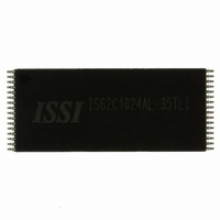
IS62C1024AL-35TLI ISSI, Integrated Silicon Solution Inc, IS62C1024AL-35TLI Datasheet

IS62C1024AL-35TLI
Specifications of IS62C1024AL-35TLI
Available stocks
Related parts for IS62C1024AL-35TLI
IS62C1024AL-35TLI Summary of contents
Page 1
... When CE1 is HIGH or CE2 is LOW (deselected), the device assumes a standby mode at which the power dissipation can be reduced by using CMOS input levels. Easy memory expansion is provided by using two Chip Enable inputs, CE1 and CE2 active LOW W rite Enable (WE) controls both writing and reading of the memory. DECODER MEMORY ARRAY I/O DATA CIRCUIT CONTROL CIRCUIT OE WE 1-800-379-4774 JULY 2008 IS62C1024AL/IS65C1024AL is a low power, 128K x 8 COLUMN I/O 1 ...
Page 2
... L 2 PIN CONFIGURATION 32-Pin TSOP (Type 1) A11 A13 CE2 6 A15 A16 10 A14 11 A12 OPERATING RANGE (IS62C1024AL) Range Commercial 0°C to +70°C Industrial OPERATING RANGE (IS65C1024AL) Range Automotive CE2 I/O Operation High High High out Integrated Silicon Solution, Inc. — www.issi.com — ...
Page 3
... IS62C1024AL IS65C1024AL ABSOLUTE MAXIMUM RATINGS Symbol Parameter V Terminal Voltage with Respect to GND term t Storage Temperature stg P Power Dissipation Output Current (LOW) out Notes: 1. Stress greater than those listed under ABSOLUTE MAXIMUM RATINGS may cause permanent damage to the device. This is a stress rating only and functional operation of the device at these or any other conditions above those indicated in the operational sections of this specification is not implied. Exposure to absolute maximum rating conditions for extended periods may affect reli- ability. CAPACITANCE (1,2) Symbol Parameter c Input Capacitance In c Output Capacitance out Notes: 1 ...
Page 4
... IS62C1024AL IS65C1024AL IS62C1024AL/IS65C1024AL POWER SUPPLY CHARACTERISTICS Symbol Parameter Test Conditions I Average operating CE1 = V cc Current Dynamic Operating Supply Current I out V In CE2 = V I TTL Standby Current (TTL Inputs or CE2 ≤ CMOS Standby Current (CMOS Inputs) CE1 ≥ V ce2 ≤ 0.2V Note address and data inputs are cycling at the maximum frequency means no input lines change. max 2 ...
Page 5
... IS62C1024AL IS65C1024AL AC TEST CONDITIONS Parameter Input Pulse Level Input Rise and Fall Times Input and Output Timing and Reference Level Output Load See Figures 1a and 1b AC TEST LOADS 1838 Ω 5V OUTPUT 100 pF Including jig and scope Figure 1a. AC WAVEFORMS READ CYCLE NO. 1 (1,2) ADDRESS DOUT Integrated Silicon Solution, Inc. — www.issi.com — Rev. H 06/26/08 Unit ...
Page 6
... IS62C1024AL IS65C1024AL READ CYCLE NO. 2 (1,3) ADDRESS OE CE1 CE2 DOUT Notes HIGH for a Read Cycle. 2. The device is continuously selected. OE, CE1 = V 3. Address is valid prior to or coincident with CE1 LOW and CE2 HIGH transitions. WRITE CYCLE SWITCHING CHARACTERISTICS Symbol Parameter t Write Cycle Time wc t CE1 to Write End 1 sce t CE2 to Write End 2 sce t Address Setup Time to Write End aw t Address Hold from Write End ha t Address Setup Time sa t (4) ...
Page 7
... IS62C1024AL IS65C1024AL AC WAVEFORMS WRITE CYCLE NO. 1 (WE Controlled) ADDRESS CE1 CE2 DOUT DATA UNDEFINED DIN WRITE CYCLE NO. 2 (CE1, CE2 Controlled) ADDRESS t SA CE1 CE2 WE DOUT DATA UNDEFINED DIN Notes: 1. The internal write time is defined by the overlap of CE1 LOW, CE2 HIGH and WE LOW. All signals must be in valid states to initiate a Write, but any one can go inactive to terminate the Write. The Data Input Setup and Hold timing are referenced to the rising or falling edge of the signal that terminates the Write ...
Page 8
... IS62C1024AL IS65C1024AL DATA RETENTION SWITCHING CHARACTERISTICS Symbol Parameter V V for Data Retention Data Retention Current Dr t Data Retention Setup Time See Data Retention Waveform sDr t Recovery Time rDr Note: 1. Typical Values are measured 5V DATA RETENTION WAVEFORM (CE1 Controlled) VDD 4.5V 2. CE1 GND DATA RETENTION WAVEFORM (CE2 Controlled) VDD 4.5V CE2 2. 0.4V GND 8 Test Condition See Data Retention Waveform V = 2.0V, CE1 ≥ ...
Page 9
... IS62C1024AL-35T Industrial Range: –40°C to +85°C Speed (ns) Order Part No. 35 IS62C1024AL-35QI 35 IS62C1024AL-35QLI 35 IS62C1024AL-35TI 35 IS62C1024AL-35TLI ORDERING INFORMATION: IS65C1024AL Automotive Range: -40°C to +125°C Speed (ns) Order Part No. 45 IS65C1024AL-45QA3 Plastic SOP 45 IS65C1024AL-45QLA3 Plastic SOP, Lead-free 45 IS65C1024AL-45TA3 45 IS65C1024AL-45TLA3 TSOP, Type 1, Lead-free Integrated Silicon Solution, Inc. — www.issi.com — ...
Page 10
... IS62C1024AL IS65C1024AL 10 Integrated Silicon Solution, Inc. — www.issi.com — 1-800-379-4774 Rev. H 06/26/08 ...
Page 11
... IS62C1024AL IS65C1024AL Integrated Silicon Solution, Inc. — www.issi.com — Rev. H 06/26/08 1-800-379-4774 11 ...


