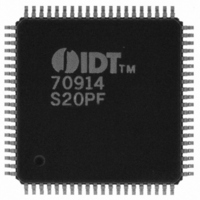
IDT70914S20PF IDT, Integrated Device Technology Inc, IDT70914S20PF Datasheet - Page 10

IDT70914S20PF
Manufacturer Part Number
IDT70914S20PF
Description
IC SRAM 36KBIT 20NS 80TQFP
Manufacturer
IDT, Integrated Device Technology Inc
Specifications of IDT70914S20PF
Format - Memory
RAM
Memory Type
SRAM - Dual Port, Synchronous
Memory Size
36K (4K x 9)
Speed
20ns
Interface
Parallel
Voltage - Supply
4.5 V ~ 5.5 V
Operating Temperature
0°C ~ 70°C
Package / Case
80-TQFP, 80-VQFP
Density
36Kb
Access Time (max)
20ns
Sync/async
Synchronous
Architecture
SDR
Clock Freq (max)
50MHz
Operating Supply Voltage (typ)
5V
Address Bus
12b
Package Type
TQFP
Operating Temp Range
0C to 70C
Number Of Ports
2
Supply Current
290mA
Operating Supply Voltage (min)
4.5V
Operating Supply Voltage (max)
5.5V
Operating Temperature Classification
Commercial
Mounting
Surface Mount
Pin Count
80
Word Size
9b
Number Of Words
4K
Lead Free Status / RoHS Status
Contains lead / RoHS non-compliant
Other names
70914S20PF
800-1370
800-1370
Available stocks
Company
Part Number
Manufacturer
Quantity
Price
Company:
Part Number:
IDT70914S20PF
Manufacturer:
IDT, Integrated Device Technology Inc
Quantity:
10 000
Company:
Part Number:
IDT70914S20PF8
Manufacturer:
IDT, Integrated Device Technology Inc
Quantity:
10 000
Functional Description
interface. Registered inputs provide very short set-up and hold times on
address, data, and all critical control inputs. All internal registers are clocked
on the rising edge of the clock signal. An asynchronous output enable is
provided to ease asynchronous bus interfacing.
Truth Table I: Read/Write Control
Truth Table II: Clock Enable Function Table
NOTES:
1. 'H' = HIGH voltage level steady state, 'h' = HIGH voltage level one set-up time prior to the LOW-to-HIGH clock transition, 'L' = LOW voltage level steady state 'l' = LOW
2. CLKEN = V
3. Control signals are initialted and terminated on the rising edge of the CLK, depending on their input level. When R/W and CE are LOW, a write cycle is initiated on
4. The register outputs are internal signals from the register inputs being clocked in or disabled by CLKEN.
IDT70914S
High-Speed 36K (4K x 9) Synchronous Dual-Port Static RAM
CLK
voltage level one set-up time prior to the LOW-to-HIGH clock transition, 'X' = Don't care, 'NC' = No change
the LOW-to-HIGH transition of the CLK. Termination of a write cycle is done on the next LOW-to-HIGH transistion of the CLK.
The IDT70914 provides a true synchronous Dual-Port Static RAM
The internal write pulse width is dependent on the LOW to HIGH
↑
↑
↑
↑
Synchronous
Hold (do nothing)
Load "1"
Load "0"
CE
Mode
H
X
IL
L
L
must be clocked in during Power-Up.
(3)
R/W
Inputs
X
H
X
L
Asynchronous
CLK
OE
X
X
L
H
↑
↑
↑
X
(3)
Inputs
DATA
Outputs
DATA
High-Z
High-Z
CLKEN
I/O
0-8
H
H
OUT
L
L
IN
(2)
Deselected, Power-Down
Selected and Write Enabled
Read Selected and Data Output Enable Read
Outputs Disabled
(1)
6.42
10
transitions of the clock signal allowing the shortest possible realized cycle
times. Clock enable inputs are provided to stall the operation of the address
and data input registers without introducing clock skew for very fast
interleaved memory applications.
internal circuitry to reduce static power consumption.
ADDR
X
X
H
L
A HIGH on the CE input for one clock cycle will power down the
Register Inputs
Military, Industrial and Commercial Temperature Ranges
(1)
DATAIN
X
X
H
L
Mode
ADDR
NC
NC
H
L
Register Outputs
DATAOUT
(4)
NC
NC
H
L
3490 tbl 10
3490 tbl 09


