MT48LC8M16LFB4-8 IT:G Micron Technology Inc, MT48LC8M16LFB4-8 IT:G Datasheet - Page 7
MT48LC8M16LFB4-8 IT:G
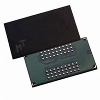
Manufacturer Part Number
MT48LC8M16LFB4-8 IT:G
Description
IC SDRAM 128MBIT 125MHZ 54VFBGA
Manufacturer
Micron Technology Inc
Type
Mobile SDRAMr
Specifications of MT48LC8M16LFB4-8 IT:G
Format - Memory
RAM
Memory Type
Mobile SDRAM
Memory Size
128M (8Mx16)
Speed
125MHz
Interface
Parallel
Voltage - Supply
3 V ~ 3.6 V
Operating Temperature
-40°C ~ 85°C
Package / Case
54-VFBGA
Organization
8Mx16
Density
128Mb
Address Bus
14b
Access Time (max)
19/8/7ns
Maximum Clock Rate
125MHz
Operating Supply Voltage (typ)
3.3V
Package Type
VFBGA
Operating Temp Range
-40C to 85C
Operating Supply Voltage (max)
3.6V
Operating Supply Voltage (min)
3V
Supply Current
100mA
Pin Count
54
Mounting
Surface Mount
Operating Temperature Classification
Industrial
Lead Free Status / RoHS Status
Lead free / RoHS Compliant


Figure 2:
PDF: 09005aef807f4885/Source: 09005aef8071a76b
128Mbx16x32Mobile_2.fm - Rev. L 10/07 EN
BA0, BA1
A0-A11,
CAS#
RAS#
WE#
CKE
CLK
CS#
14
ADDRESS
REGISTER
Functional Block Diagram 8 Meg x 16 SDRAM
MODE REGISTER
CONTROL
LOGIC
12
The 128Mb SDRAM device uses an internal pipelined architecture to achieve high-speed
operation. This architecture is compatible with the 2n rule of prefetch architectures, but
it also enables the column address to be changed on every clock cycle to achieve a high-
speed, fully random access. Precharging one bank while accessing one of the other three
banks will hide the precharge cycles and provide seamless high-speed, random-access
operation.
The 128Mb SDRAM device is designed to operate in 3.3V or 2.5V low-power memory
systems. The 2.5V version is compatible with 1.8V I/O interface. An auto refresh mode is
provided along with a power-saving, power-down mode. All inputs and outputs are
LVTTL-compatible.
SDRAMs offer substantial advances in DRAM operating performance, including the
ability to synchronously burst data at a high data rate with automatic column-address
generation, the ability to interleave between internal banks to hide precharge time, and
the capability to randomly change column addresses on each clock cycle during a burst
access.
COUNTER
REFRESH
12
9
2
12
ADDRESS
2
ROW-
MUX
COUNTER/
COLUMN-
CONTROL
ADDRESS
LATCH
BANK
LOGIC
12
DECODER
ADDRESS
BANK0
LATCH
ROW-
&
9
7
4096
READ DATA LATCH
SENSE AMPLIFIERS
DQM MASK LOGIC
(4,096 x 512 x 16)
WRITE DRIVERS
I/O GATING
DECODER
COLUMN
MEMORY
Micron Technology, Inc., reserves the right to change products or specifications without notice.
BANK0
ARRAY
4,096
(x16)
512
BANK1
BANK2
128Mb: x16, x32 Mobile SDRAM
BANK3
16
16
2
General Description
©2001 Micron Technology, Inc. All rights reserved.
REGISTER
REGISTER
OUTPUT
DATA
DATA
INPUT
2
16
DQML,
DQMH
DQ0-
DQ15
Related parts for MT48LC8M16LFB4-8 IT:G
Image
Part Number
Description
Manufacturer
Datasheet
Request
R

Part Number:
Description:
IC SDRAM 64MBIT 133MHZ 54TSOP
Manufacturer:
Micron Technology Inc
Datasheet:

Part Number:
Description:
IC SDRAM 64MBIT 5.5NS 86TSOP
Manufacturer:
Micron Technology Inc
Datasheet:
Part Number:
Description:
IC SDRAM 64MBIT 200MHZ 86TSOP
Manufacturer:
Micron Technology Inc
Datasheet:
Part Number:
Description:
IC SDRAM 64MBIT 133MHZ 54TSOP
Manufacturer:
Micron Technology Inc
Datasheet:
Part Number:
Description:
IC SDRAM 128MBIT 133MHZ 54TSOP
Manufacturer:
Micron Technology Inc
Datasheet:

Part Number:
Description:
IC SDRAM 256MBIT 133MHZ 90VFBGA
Manufacturer:
Micron Technology Inc
Datasheet:
Part Number:
Description:
IC SDRAM 128MBIT 133MHZ 54TSOP
Manufacturer:
Micron Technology Inc
Datasheet:
Part Number:
Description:
IC SDRAM 256MBIT 133MHZ 54TSOP
Manufacturer:
Micron Technology Inc
Datasheet:

Part Number:
Description:
IC DDR SDRAM 512MBIT 6NS 66TSOP
Manufacturer:
Micron Technology Inc
Datasheet:
Part Number:
Description:
IC SDRAM 128MBIT 167MHZ 86TSOP
Manufacturer:
Micron Technology Inc
Datasheet:
Part Number:
Description:
IC SDRAM 128MBIT 143MHZ 86TSOP
Manufacturer:
Micron Technology Inc
Datasheet:

Part Number:
Description:
SDRAM 256M-BIT 1.8V 54-PIN VFBGA
Manufacturer:
Micron Technology Inc
Datasheet:
Part Number:
Description:
IC SDRAM 128MBIT 143MHZ 86TSOP
Manufacturer:
Micron Technology Inc
Datasheet:

Part Number:
Description:
IC SDRAM 128MBIT 125MHZ 54VFBGA
Manufacturer:
Micron Technology Inc
Datasheet:
Part Number:
Description:
IC SDRAM 128MBIT 125MHZ 54VFBGA
Manufacturer:
Micron Technology Inc
Datasheet: