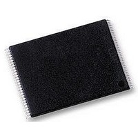
NAND256W3A2BN6E NUMONYX, NAND256W3A2BN6E Datasheet - Page 24

NAND256W3A2BN6E
Manufacturer Part Number
NAND256W3A2BN6E
Description
IC FLASH 256MBIT 48TSOP
Manufacturer
NUMONYX
Datasheet
1.NAND128W3A2BN6E.pdf
(59 pages)
Specifications of NAND256W3A2BN6E
Format - Memory
FLASH
Memory Type
FLASH - Nand
Memory Size
256M (32M x 8)
Interface
Parallel
Voltage - Supply
2.7 V ~ 3.6 V
Operating Temperature
-40°C ~ 85°C
Package / Case
48-TSOP
Access Time
12µs
Supply Voltage Range
1.7V To 1.95V, 2.7V To 3.6V
Memory Case Style
TSOP
No. Of Pins
48
Base Number
256
Block Size
16896Byte
Memory Configuration
32k X 8
Rohs Compliant
Yes
Lead Free Status / RoHS Status
Lead free / RoHS Compliant
Speed
-
Lead Free Status / RoHS Status
Lead free / RoHS Compliant, Lead free / RoHS Compliant
Other names
497-5038
497-5038
497-5038
Available stocks
Company
Part Number
Manufacturer
Quantity
Price
Company:
Part Number:
NAND256W3A2BN6E
Manufacturer:
ST
Quantity:
11 245
Company:
Part Number:
NAND256W3A2BN6E
Manufacturer:
MICRON/EOL43
Quantity:
444
Part Number:
NAND256W3A2BN6E
Manufacturer:
ST
Quantity:
20 000
Device operations
6.2
24/59
Figure 9.
Read memory array
Each operation to read the memory area starts with a pointer operation as shown in the
Section 6.1: Pointer
Read A, Read B or Read C commands three bus cycles are required to input the address of
the data to be read.
The device defaults to Read A mode after power-up or a reset operation.
When reading the following spare area addresses:
set the start address of the spare area, while the following addresses are ignored:
Once the Read A or Read C commands have been issued they do not need to be reissued
for subsequent read operations as the pointer remains in the respective area. However, the
Read B command is effective for only one operation; once an operation has been executed
in Area B the pointer returns automatically to Area A. Another Read B command is required
to start another read operation in Area B.
Once a read command is issued two types of operations are available: random read and
page read.
I/O
I/O
I/O
Areas B, C can be programmed depending on how much data is input. The 01h command must be re-issued before each program.
A0 to A3 (x8 devices)
A0 to A2 (x16 devices)
A4 to A7 (x8 devices)
A3 to A7 (x16 devices)
Random read
Each time the command is issued the first read is random read.
Page read
After the random read access the page data is transferred to the page buffer in a time
of t
transfer is complete the Ready/Busy signal goes High. The data can then be read out
sequentially (from the selected column address to the last column address) by pulsing
the Read Enable signal.
Sequential row read
After the data in last column of the page is output, if the Read Enable signal is pulsed
Areas A, B, C can be programmed depending on how much data is input. Subsequent 00h commands can be omitted.
WHBH
00h
01h
50h
Pointer operations for programming
(refer to
80h
80h
80h
Only Areas C can be programmed. Subsequent 50h commands can be omitted.
operations. Once the area (main or spare) has been selected using the
Address
Address
Address
Table 20: AC characteristics for operations
Inputs
Inputs
Inputs
Data Input
Data Input
Data Input
10h
10h
10h
AREA A
AREA B
AREA C
00h
01h
50h
80h
80h
80h
Address
Address
Address
Inputs
Inputs
Inputs
NAND128-A, NAND256-A
for the value). Once the
Data Input
Data Input
Data Input
10h
10h
10h
ai07591


