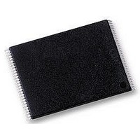
NAND256W3A2BN6E NUMONYX, NAND256W3A2BN6E Datasheet - Page 32

NAND256W3A2BN6E
Manufacturer Part Number
NAND256W3A2BN6E
Description
IC FLASH 256MBIT 48TSOP
Manufacturer
NUMONYX
Datasheet
1.NAND128W3A2BN6E.pdf
(59 pages)
Specifications of NAND256W3A2BN6E
Format - Memory
FLASH
Memory Type
FLASH - Nand
Memory Size
256M (32M x 8)
Interface
Parallel
Voltage - Supply
2.7 V ~ 3.6 V
Operating Temperature
-40°C ~ 85°C
Package / Case
48-TSOP
Access Time
12µs
Supply Voltage Range
1.7V To 1.95V, 2.7V To 3.6V
Memory Case Style
TSOP
No. Of Pins
48
Base Number
256
Block Size
16896Byte
Memory Configuration
32k X 8
Rohs Compliant
Yes
Lead Free Status / RoHS Status
Lead free / RoHS Compliant
Speed
-
Lead Free Status / RoHS Status
Lead free / RoHS Compliant, Lead free / RoHS Compliant
Other names
497-5038
497-5038
497-5038
Available stocks
Company
Part Number
Manufacturer
Quantity
Price
Company:
Part Number:
NAND256W3A2BN6E
Manufacturer:
ST
Quantity:
11 245
Company:
Part Number:
NAND256W3A2BN6E
Manufacturer:
MICRON/EOL43
Quantity:
444
Part Number:
NAND256W3A2BN6E
Manufacturer:
ST
Quantity:
20 000
Software algorithms
7
7.1
7.2
32/59
Software algorithms
This section gives information on the software algorithms that Numonyx recommends to
implement to manage the bad blocks and extend the lifetime of the NAND device.
NAND flash memories are programmed and erased by Fowler-Nordheim tunneling using a
high voltage. Exposing the device to a high voltage for extended periods can cause the
oxide layer to be damaged. For this reason, the number of program and erase cycles is
limited (see
values) and it is recommended to implement garbage collection, a wear-leveling algorithm
and an error correction code to extend the number of program and erase cycles and
increase the data retention.
For the integration of NAND memories into an application, Numonyx provides a full range of
software solutions such as file systems, sector managers, drivers, and code management.
Contact the nearest Numonyx sales office or visit www.numonyx.com for more details.
Bad block management
Devices with bad blocks have the same quality level and the same AC and DC
characteristics as devices where all the blocks are valid. A bad block does not affect the
performance of valid blocks because it is isolated from the bit line and common source line
by a select transistor.
The devices are supplied with all the locations inside valid blocks erased (FFh). The bad
block information is written prior to shipping. Any block where the 6th byte (x8 devices)/1st
word (x16 devices), in the spare area of the 1st page, does not contain FFh is a bad block.
The bad block information must be read before any erase is attempted as the bad block
information may be erased. For the system to be able to recognize the bad blocks based on
the original information it is recommended to create a bad block table following the flowchart
shown in
Block replacement
Over the lifetime of the device additional bad blocks may develop. In this case the block has
to be replaced by copying the data to a valid block. These additional bad blocks can be
identified as attempts to program or erase them outputs errors to the status register.
As the failure of a page program operation does not affect the data in other pages in the
same block, the block can be replaced by re-programming the current data and copying the
rest of the replaced block to an available valid block. The Copy Back Program command can
be used to copy the data to a valid block.
Refer to
Section 6.4: Copy back program
Figure 17: Bad block management
Table 14: Program, erase times and program erase endurance cycles
for more details.
flowchart.
NAND128-A, NAND256-A
for the


