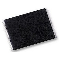
NAND256W3A2BN6E NUMONYX, NAND256W3A2BN6E Datasheet - Page 58

NAND256W3A2BN6E
Manufacturer Part Number
NAND256W3A2BN6E
Description
IC FLASH 256MBIT 48TSOP
Manufacturer
NUMONYX
Datasheet
1.NAND128W3A2BN6E.pdf
(59 pages)
Specifications of NAND256W3A2BN6E
Format - Memory
FLASH
Memory Type
FLASH - Nand
Memory Size
256M (32M x 8)
Interface
Parallel
Voltage - Supply
2.7 V ~ 3.6 V
Operating Temperature
-40°C ~ 85°C
Package / Case
48-TSOP
Access Time
12µs
Supply Voltage Range
1.7V To 1.95V, 2.7V To 3.6V
Memory Case Style
TSOP
No. Of Pins
48
Base Number
256
Block Size
16896Byte
Memory Configuration
32k X 8
Rohs Compliant
Yes
Lead Free Status / RoHS Status
Lead free / RoHS Compliant
Speed
-
Lead Free Status / RoHS Status
Lead free / RoHS Compliant, Lead free / RoHS Compliant
Other names
497-5038
497-5038
497-5038
Available stocks
Company
Part Number
Manufacturer
Quantity
Price
Company:
Part Number:
NAND256W3A2BN6E
Manufacturer:
ST
Quantity:
11 245
Company:
Part Number:
NAND256W3A2BN6E
Manufacturer:
MICRON/EOL43
Quantity:
444
Part Number:
NAND256W3A2BN6E
Manufacturer:
ST
Quantity:
20 000
Revision history
58/59
Table 24.
23-June-2005
13-Dec-2004
25-Feb-2005
09-Aug-2005
13-Aug-2008
30-Nov-2009
20-Jun-2008
Date
Document revision history (continued)
Version
10
11
12
13
14
15
16
R
Section 1:
WSOP48 replaced with USOP48 package,
VFBGA63 (8.5 x 15 x 1mm) replaced with VFBGA63 (9 x 11 x 1mm)
package,
TFBGA63 (8.5 x 15 x 1mm) replaced with TFBGA63 (9 x 11 x 1.2mm)
package.
Changes to
t
packages removed throughout document. Sequential row read removed
throughout document.
T
protection
characteristics measurement
Modified
Section 6.2: Read memory
Section 6.8: Read electronic
management
Figure 10: Read (A, B, C) operations
signature AC waveform
Note added to
TSOP48 connections, x16 devices
Removed all information pertaining to the 512-Mbit and 1-Gbit devices.
Applied Numonyx branding.
Removed all the information pertaining the 1.8 V devices (V
1.95 V) and the USOP48 and VFBGA63 packages. Added the sequential
row read option throughout the document.
Added security features on the cover page and in
Updated
value versus waveform timings for Ready/Busy
ECOPACK removed and replaced by RoHS compliance. Modified
dimension A2 of the VFBGA55 package in
testing option in
EHBH
EHQX and
ref
,
parameter added to the description of the family clarified in the
t
EHEL
,
Section 3.7: Write Enable
Figure 32: Ready/Busy AC waveform
t
T
section and
Description.
RHBL
RHQX
Table 20: AC characteristics for
and
removed throughout document. TFBGA63 and TFBGA55
Figure 3: TSOP48 connections, x8 devices
Table 23: Ordering information
added throughout document.
Section 12: Ordering
Figure 20: Equivalent testing circuit for AC
modified.
array,
Revision details
signature,
added.
Section 6.3: Page
regarding the USOP package.
(W),
and
Section 7.1: Bad block
information.
Section 3.5: Chip Enable
Figure 26: Read electronic
Table
operations.
NAND128-A, NAND256-A
and
Section 10.2: Data
signal. References to
scheme.
22. Added automotive
Section 1:
Figure 34: Resistor
program,
and
DD
Description.
Figure 4:
= 1.7 to
(E),


